
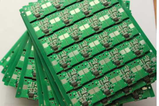
Professional PCB manufacturing and assembly
Building 6, Zone 3, Yuekang Road,Bao'an District, Shenzhen, China
+86-13410863085Mon.-Sat.08:00-20:00

In the PCB design process, some circuit boards will be involved in the calculation of impedance values. kingford will introduce the impedance calculation method using polar tool. Take a four-layer board as an example. The general layers of four-layer board are top, gnd02, power03 and bottom. From the point of view of the four-layer plate is composed of two signal layers and plane layer. The following will explain how to calculate the impedance value of PCB design and PCB copy board design to meet the challenges related knowledge.
1. How does PCB copy board design meet the challenges
Under the influence of the policies of the National Two Sessions to support entrepreneurship and innovation, the local electronics industry has accelerated the transformation and the opening of the smart era. In this great era of intelligence, PCB copy board design technology upgrade is essential. With the expansion of the smartphone and tablet market, the emergence of portable terminals, and the development of in-vehicle, medical and access devices in emerging markets, products want to be thinner and lighter, want to increase the speed of communication, want to achieve all kinds of communication simultaneously, want to achieve long battery life, and bring products to market faster than competitors. These need to copy PCB board, design and manufacturing put forward higher requirements, in order to cope with the intelligent era of the ever-changing challenges.
The advent of the intelligent era has not only brought convenience to the lives of ordinary people, but also had a profound impact on various industries. In order to make PCB have high reliability, it is necessary to put forward higher requirements for PCB copy board and design. For example, intelligent products require device quality, density heat dissipation, ubiquitous Internet of Things communication, and intelligent production requires flexible equipment, intelligent machinery, complex environment, and so on. These factors should be taken into account in PCB copying board design, professional PCB copying board companies should continue to improve precision PCB copying board, flexible circuit board copying board, EMC design, SI high-speed design and other technical services. What is the role of PCB board copying software in intelligent product board copying design?
Is it a tool to reverse extract PCB files? Is it a container for the backwards schematic? Is the product BOM list management system? PCB board copy software in the changing technological innovation, and how to conform to the trend of The Times, help the new generation of intelligent product board copy design? "From 2D design to 3DPCB design, from simple double panel copying board, to high density multi-layer copying board... None of these simple changes represent the future of PCB board design." Longren PCB copying board expert said, "to solve the current PCB copying board software real 'pain' is to achieve fully customized services, constantly improve the efficiency of research and development." Good PCB copying design starts with adequate DRC checking in the layout tool.
As PCB design in today's smart age becomes more complex, so does DRC inspection, and there is often a huge gap between layout designers and board copying engineers, who have different design expertise, use different tools, and use different units of measurement. ERC/SRC (Electrical Rule/Simulation Rule) checks fill the gap. In short, the intelligent era, the complexity of PCB design will continue to improve, simple PCB copy board cloning has been difficult to meet the design requirements, PCB copy board positive and reverse research one-stop service system has become a trend, PCB copy board should be integrated into the whole industry chain, close to customer needs, to achieve fully customized services and so on.

2. How to calculate impedance value in PCB design
1. Open the impedance calculation tool of polar company as shown in the following figure: We first select the template. Since there are two signal plus planes, we only need to calculate one signal plus plane.
2. The next step is the selection of parameters. Generally, the impedance of single line is 50 ohm, the impedance of differential line is 100 ohm, H is the height of insulating medium,W,W1 is the line width, and T is the copper thickness (the copper thickness of inner layer is generally 1.4MIL, and the copper thickness of TOP and BOTTOM layer is generally 2.0mil). Dielectric (FR-4)Er is generally 4.3. The single-line impedance is determined first and then the differential line impedance is calculated, as shown in the figure below
3. After calculating the height of a single line, then calculate the impedance of the difference line. The difference line template is as follows: In the figure above, S is the distance between the difference lines (note S< 2W), calculate the impedance of the difference line as shown below,
4. After the impedance of single line and difference line is calculated, the next step is to calculate the laminated thickness, assuming that the customer gives the plate thickness of 1.6mm.
Generally, 1.7mil is used to calculate the thickness of the TOP and Bottom layers in the following figure, because that is related to the smallest hole and plate thickness, and the manufacturer, of course, if the current is too large, it will be thicker. The thickness of the intermediate layer, if the current to be passed through is normal, will generally choose 35um. The differential impedance is also chosen in a similar way. coupled coated microstrip and edge-coupled offset microstrip are also calculated with the one with cover on top and the one with asymmetric middle. A little note, generally four layers of plate only a medium layer, two layers of PC material,(plate factory default laminating process) so the dielectric constant is not the same.

How to quickly inspect the circuit board
Feb 06,2023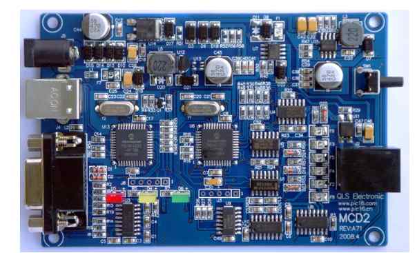


Just upload Gerber files, BOM files and design files, and the KINGFORD team will provide a complete quotation within 24h.