
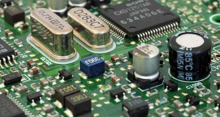
Professional PCB manufacturing and assembly
Building 6, Zone 3, Yuekang Road,Bao'an District, Shenzhen, China
+86-13410863085Mon.-Sat.08:00-20:00


Slotting is a common structure in PCB design. We often say that the "cross partition problem" is actually a slot problem.
One, the generation of grooving
The generation of slotting can be summarized into the following two cases.
(1) Slot caused by power supply/ground plane division
When there are a variety of different power sources or ground on the PCB board, it is generally impossible to allocate a complete plane for each power network and ground network. The common practice is to divide the power source or ground on one or more planes. Grooves are formed between different segments on the same plane.
(2) The through hole is too dense to form grooves
The through hole comprises a pad and a through hole. When the through hole passes through the stratum or power layer without electrical connection to it, some space (i.e. isolation ring) should be left around the through hole for electrical isolation. But when the through-holes are too close together, the isolation rings overlap, creating grooves. This is also known as the hot pad problem.
Second, the influence of slotting on EMC performance of printed circuit board
The slotting will affect the EMC performance of PCB board. This effect can be either negative or positive.
(1) Surface current distribution of high-speed signal and low-speed signal
At low speeds, the current flows along the path with the lowest resistance.
At high speeds, the effect of inductance on the signal return path will outweigh the effect of resistance. The high-speed return signal will flow along the path with the lowest impedance.
(2) The concept of "land division"
When incompatible circuits exist on the PCB circuit board, ground cables need to be set according to different power voltage, digital and analog signals, high-speed and low-speed signals, and high-current and low-current signals.
The function of ground division can be easily understood from the distribution of the backflow of high speed signals and low speed signals given above: Ground division can prevent the superposition of the backflow signals of incompatible circuits and prevent the coupling of common ground impedance.
Two things to note:
First, the concept of ground division is different from the "problem of signal crossing the power plane or the slot on the ground plane" discussed below. Ground division is just to set the ground wire (or plane) respectively according to different kinds of signals:
Second, the subdivision does not completely isolate all kinds of land without any electrical connection. After subdivision, all kinds of land will be connected at appropriate positions to ensure the electrical continuity of the whole stratum.
(3) Signal across the power plane or ground level slot problem
Both high - speed and low - speed signals should not be routed across the division. There are a number of serious problems associated with straddling, including:
1. Increase the current loop area, increase the loop inductance, so that the output waveform is easy to oscillate;
2. Increased radiation interference to space, while susceptible to the influence of space magnetic field;
3. Increase the possibility of magnetic coupling with other circuits on the board;
4. The high frequency voltage drop on the loop inductance constitutes the common-mode radiation source and generates common-mode radiation through the external cable.
For high-speed signals that require strict impedance control and follow the strip-line model, the strip-line model will also be damaged due to the slotting of the upper or lower planes, resulting in impedance discontinuity and serious signal integrity problems.
Three, slotting treatment
Grooving should be handled according to the following principles
(1) High-speed signal lines requiring strict impedance control shall be strictly prohibited from crossing the division
Cross-segment routing can cause impedance discontinuity and serious signal integrity problems.
(2) When there is incompatible circuit on the PCB board, it should be processed by land division
Ground division should not cause the cross-division of high-speed signal lines, and try not to cause the cross-division of low-speed signal lines.
(3) When cross-slotted routing is unavoidable, bridge should be carried out
When the signal line cannot avoid the situation of crossing the slot, it should be effectively bridged to connect the ground plane meters along the direction of the signal path.
(4) The connector (external) should not be placed on the stratigraphic separation
(5) Processing of high-density connectors
High-density connectors (such as the 2mm connector widely used today) will create grooves if the radius of the isolation ring is too large when passing through the power supply and ground plane. In PCB design, unless there are special requirements (such as strict safety distance requirements for individual signals), it is generally necessary to ensure that the ground network encircles each pin. The ground network can also be evenly arranged during pin layout to ensure the continuity of the ground plane and prevent the occurrence of slot.
(6) Processing across "static" segmentation
When I/O signals are screened and filtered out of the sub-rack or cabinet through cables, a clean ground is required that is not polluted by internal noise.
Without this piece of "static", the high-frequency signal filtering has little effect. A "quiet place" can be a metal frame or a protective place. Static is not connected to the logical ground inside the board.
When the "static" is set on the PCB board, the I/O signal cables inevitably need to be routed across the "static" division. You need to do something about it.
For differential signal lines, common mode noise can be effectively suppressed by "static" routing across the lines without any processing.


Just upload Gerber files, BOM files and design files, and the KINGFORD team will provide a complete quotation within 24h.