
Professional PCB manufacturing and assembly
Building 6, Zone 3, Yuekang Road,Bao'an District, Shenzhen, China
+86-13410863085Mon.-Sat.08:00-20:00

For customers, what are the most concerned factors of PCB proofing?
Step 1: Speed
PCB proofing industry, time is a very important factor. Delivery time and quality are the hard strength of the factory, but also the most favored purchasing customers. Now PCB proofing factories generally provide expedited service, such as 12 hours, 24 hours expedited delivery; Usually the normal delivery time of single and double panels is 2 days.
Step 2: Quality
PCB proofing, quality can not be ignored. From raw materials, drawing, to production, testing, quality control, and so on, every link needs to be strictly checked. Take the common double panel for example, the board generally has FR-4, aluminum substrate, CEM-1, plate thickness from 0.4mm to 3.0m, copper thickness 0.5oz to 3.0oz, the difference in these materials caused by the price differentiation is very big, the manufacturers use the better material is imported plate.
Step 3: Price
With the development of the industry, the price of PCB proofing, small and medium-sized batch production is constantly falling. Complete challenging tasks with challenging prices, which will be the price trend of PCB proofing in the future.

How to achieve high PCB spread rate and shorten the design time, which is a lot of people are considering the problem, this time, long Bo technology and you discuss the design skills of pcb board layout.
Layout of circuit board copying board components:
1. In the process of optimal assembly, manufacturability design rules will restrict the layout of pcb board copying components. If the assembly department allows the components to move, the circuit can be optimized for automatic wiring.
2. In the layout of pcb circuit board, the power decoupling circuit should be designed near the relevant circuit, rather than placed in the power supply part, otherwise it will not only affect the bypass effect, but also flow pulsating current above the power line and ground wire, causing interference;
3. For the power supply direction inside the circuit, power supply should be taken from the final stage to the forward stage, and the power filter capacitor of the pcb circuit board is arranged near the final stage;
4, we should pay attention to the voltage control pcb circuit board copy board power supply in the layout, as far as possible arranged in a separate printed board. When the power supply and circuit are used together in the printed board, in the layout, the voltage regulator should avoid mixing the power supply and circuit components or making the power supply and circuit common ground.
The above is the layout of pcb board components, I hope to help you.
In order to obtain good performance of electronic circuit, component layout and wire layout are very important. In order to design a high quality and low cost pcb, what principles should be followed when determining the location of components?
The pcb board must comply with the following principles when determining component locations:
1. Shorten the connection between high-frequency components as far as possible, and try to reduce their distribution parameters and electromagnetic interference between each other. Easily disturbed components should not be too close to each other, input and output components should be as far away as possible.
2. There may be a high potential difference between some components or wires. The distance between them should be increased to avoid accidental short circuit of pcb circuit board caused by discharge. Components with high voltage should be arranged as far as possible in places that are not easily touched by the hand during debugging.
3, the weight of more than 15g components, should be fixed with a support, and then welding. Those large and heavy, heat components, should not be installed on the pcb circuit board, but should be installed on the chassis floor of the whole machine, and should consider the problem of heat dissipation. The heat sensitive element should be far away from the heating element.
4, for the potentiometer, adjustable inductor coil, variable capacitor, micro switch and other adjustable components layout should consider the structural requirements of the whole machine. If pcb circuit board machine adjustment, should be placed above the printed board for easy to adjust the place; If the outside of the machine adjustment, its position to adjust the knob on the chassis panel position.
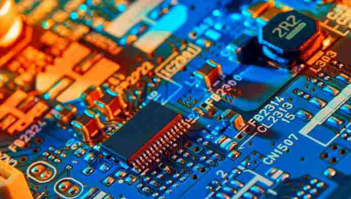
Almost every kind of electronic equipment, from small electronic watches and calculators to large computers, communication electronic equipment and military weapon systems, as long as there are electronic components such as integrated circuits, in order to make the electrical interconnection between the components, the pcb circuit board is used.
In order to obtain good performance of electronic circuit, component layout and wire layout are very important. In order to design a high quality and low cost pcb, what principles should be followed when determining the location of components?
The pcb board must comply with the following principles when determining component locations:
1. Shorten the connection between high-frequency components as far as possible, and try to reduce their distribution parameters and electromagnetic interference between each other. Easily disturbed components should not be too close to each other, input and output components should be as far away as possible.
2. There may be a high potential difference between some components or wires. The distance between them should be increased to avoid accidental short circuit of pcb circuit board caused by discharge. Components with high voltage should be arranged as far as possible in places that are not easily touched by the hand during debugging.
3, the weight of more than 15g components, should be fixed with a support, and then welding. Those large and heavy, heat components, should not be installed on the pcb circuit board, but should be installed on the chassis floor of the whole machine, and should consider the problem of heat dissipation. The heat sensitive element should be far away from the heating element.
4, for the potentiometer, adjustable inductor coil, variable capacitor, micro switch and other adjustable components layout should consider the structural requirements of the whole machine. If pcb circuit board machine adjustment, should be placed above the printed board for easy to adjust the place; If the outside of the machine adjustment, its position to adjust the knob on the chassis panel position.
Almost every kind of electronic equipment, from small electronic watches and calculators to large computers, communication electronic equipment and military weapon systems, as long as there are electronic components such as integrated circuits, in order to make the electrical interconnection between the components, the pcb circuit board is used.

PCB detailed layout, wiring design overview
Feb 04,2023


Just upload Gerber files, BOM files and design files, and the KINGFORD team will provide a complete quotation within 24h.