
Professional PCB manufacturing and assembly
Building 6, Zone 3, Yuekang Road,Bao'an District, Shenzhen, China
+86-13410863085Mon.-Sat.08:00-20:00


It is important for pcb manufacturers to share that pcba machining quality is very important, so PCBA designers need to consider this from the beginning. In some treatments, the quality of normal operation is flawed and it is easy to damage solder joints or electronic materials of machined SMT components if the initial design sketch is not suitable.
pcb manufacturers share that pcba processing should pay attention to these points:
1.BGA, chip capacitors, crystal oscillators and other stress-sensitive equipment are easily damaged by machinery or high temperature. Therefore, pcb manufacturers believe that when designing or reinforcing equipment, they should be placed on PCB boards with higher hardness, or use certain methods to avoid pcba processing.
2. When pcba processes components, it is necessary to arrange sensitive electronic components on PCB with higher stiffness. For example, in order to avoid damaging the sensitive electronic components of the PCB board during assembly, the connector that holds the PCB board and the mother board should be placed on the side of the PCB sub-board and should not be too small to the screw hole, more than 10 mm.
3.pcb manufacturer reminds that in order to avoid stress cracking of BGA solder joints, please avoid placing the BGA layout in the pcba processing and assembly process where it is easy to bend. The poor design of the BGA can easily cause the solder joints to crack if the board is held with one hand.
The above three points are mainly based on pcb manufacturers over the years of research and development and design published some discussion. In addition, it is important to reduce the pressure of assembly, adopt appropriate methods and tools, strengthen personnel training, and standardize the operation.
What are the most concerned factors of PCB proofing
For customers, what are the most concerned factors of PCB proofing?

Step 1: Speed
PCB proofing industry, time is a very important factor. Delivery time and quality are the hard strength of the factory, but also the most favored purchasing customers. Now PCB proofing factories generally provide expedited service, such as 12 hours, 24 hours expedited delivery; Usually the normal delivery time of single and double panels is 2 days.
Step 2: Quality
PCB proofing, quality can not be ignored. From raw materials, drawing, to production, testing, quality control, and so on, every link needs to be strictly checked. Take the common double panel for example, the board generally has FR-4, aluminum substrate, CEM-1, plate thickness from 0.4mm to 3.0m, copper thickness 0.5oz to 3.0oz, the difference in these materials caused by the price differentiation is very big, the manufacturers use the better material is imported plate.
Step 3: Price
With the development of the industry, the price of PCB proofing and small and medium-sized batch production is constantly decreasing. Complete challenging tasks with challenging prices, which will be the price trend of PCB proofing in the future.
In order to obtain good performance of electronic circuit, component layout and wire layout are very important. In order to design a high quality and low cost pcb, what principles should be followed when determining the location of components? Follow long Bo technology to understand!
The pcb board must comply with the following principles when determining component locations:
1. Shorten the connection between high-frequency components as far as possible, and try to reduce their distribution parameters and electromagnetic interference between each other. Easily disturbed components should not be too close to each other, input and output components should be as far away as possible.
2. There may be a high potential difference between some components or wires. The distance between them should be increased to avoid accidental short circuit of pcb circuit board caused by discharge. Components with high voltage should be arranged as far as possible in places that are not easily touched by the hand during debugging.
3, the weight of more than 15g components, should be fixed with a support, and then welding. Those large and heavy, heat components, should not be installed on the pcb circuit board, but should be installed on the chassis floor of the whole machine, and should consider the problem of heat dissipation. The heat sensitive element should be far away from the heating element.
4, for the potentiometer, adjustable inductor coil, variable capacitor, micro switch and other adjustable components layout should consider the structural requirements of the whole machine. If pcb circuit board machine adjustment, should be placed above the printed board for easy to adjust the place; If the outside of the machine adjustment, its position to adjust the knob on the chassis panel position.
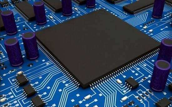
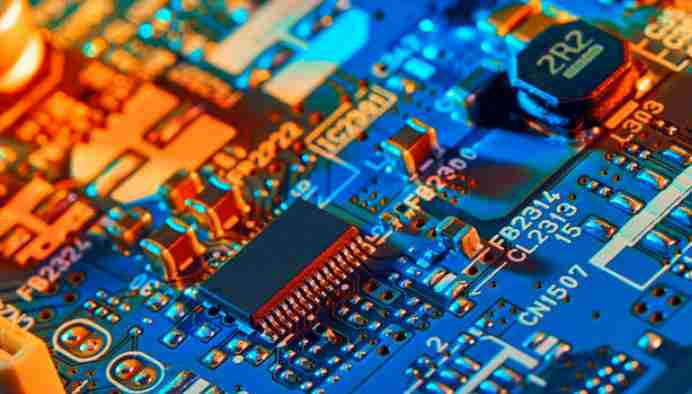
Almost every kind of electronic equipment, from small electronic watches and calculators to large computers, communication electronic equipment and military weapon systems, as long as there are electronic components such as integrated circuits, in order to make the electrical interconnection between the components, the pcb circuit board is used.


Just upload Gerber files, BOM files and design files, and the KINGFORD team will provide a complete quotation within 24h.