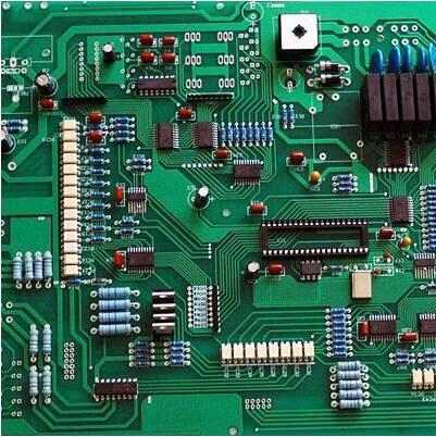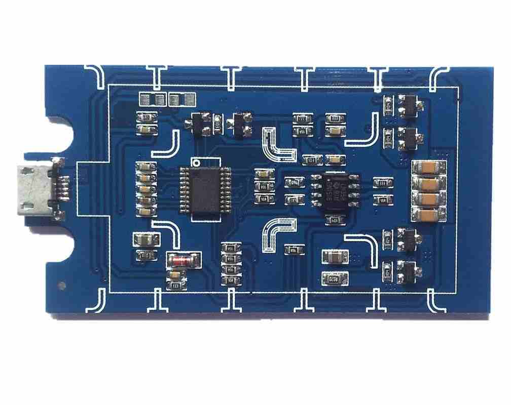
In hardware design, PCB design is a very important and indispensable step. For some simple products, the PCB design may simply connect all the components and networks accordingly. For high-speed circuit and RF circuit, PCB design directly affects whether the function of the product is normal and whether the product can meet the market requirements. The following, from the PCB design process, PCB layout, PCB wiring, PCB design checklist four aspects are introduced.
PCB design process
The quality of PCB directly determines the good and bad of an electronic product, so a good PCB design process is very important. Many engineers think of PCB design as simply laying out all the components and then connecting all the related device pins together. This is a narrow view, a good PCB design process from the principle of the scheme design has begun, such as how to choose the right scheme, choose the right electronic components and so on.
Specifically, it includes schematic design, schematic netsheet output and import, mechanical structure drawing import, cascade structure design and editing, signal integrity (SI), pre-PI simulation of power supply, PCB layout, design constraint rule import, PCB wiring, signal integrity (SI), power supply integrity (PI), electromagnetic compatibility (EMC), and post-thermal simulation Design manufacturability (DFM) check, generate production document (Gerber). The work may be done by a single engineer or by multiple engineers working together. Of course, not every product's PCB design process is the same, and specific products can be refined, added or deleted appropriately according to this process.
PCB layout
Layout is an important part of design. The result of layout will directly affect the effect of wiring, so it can be considered that a reasonable layout is the first step of successful PCB design. Simple understanding, PCB layout is to put all the components in accordance with the functional structure, modular, to meet the requirements of DXF, to meet the smooth layout and wiring principles.
Consider the overall beauty of a product is successful or not, one is to pay attention to the internal quality, two is to take into account the overall beauty, both are more perfect in order to consider the product is successful. On a PCB board, the layout of components is required to be balanced, dense and orderly, not top-heavy or heavy.
What is said above is only some big direction and requirements, in fact, PCB layout needs to take into account a lot of factors, such as often in accordance with the layout principle of "first large and then small, first to meet the structure and then to meet the beauty, first difficult and then easy", that is, the important core unit circuit, high-speed circuit, RF circuit, core components, interface circuit layout priority. And then lay out some ancillary circuits. The following principles can be followed in PCB layout design.

1. Major components should be arranged according to the principle block diagram and the main signal flow pattern of the board. The layout should meet the following requirements as far as possible:
In the absence of special requirements, make the total length of wiring as short as possible, the key signal line shortest;
The layout of the decoupling capacitor, according to the size of the capacitor as far as possible according to the smaller the capacitor closer to the IC power pin, and the circuit formed between the power supply and the ground is shortest;
Reduce the signal return path, do not appear cross-segmentation phenomenon.
2. The arrangement of components should first meet the requirements of function, but also facilitate subsequent debugging and maintenance, that is, large components can not be placed around the small components, and there should be enough space around the components to be debutted. Too compact will lead to the inability to soldering iron.
3, the same structure of the circuit, as far as possible to use "symmetrical" standard layout; Optimize the layout according to the standards of uniform distribution, balanced center of gravity and beautiful layout.
4. The plug-in components of the same type shall be placed in the same direction in the X or Y direction. The same type of polar discrete components should also be as consistent as possible in the X or Y direction, so as to facilitate production and inspection.
5, the heating element should generally be evenly distributed to facilitate the heat dissipation of the veneer and the whole machine. In addition to the temperature detection element, the temperature sensitive devices should be far away from the components with large heat. In addition to temperature sensors, triodes are also heat-sensitive devices.
6, high voltage, large current signal and small current, low voltage weak signal completely separate.
7, analog signal and digital signal separate; High frequency signals are separated from low frequency signals; The spacing of high-frequency components should be sufficient.
8, component layout, should be appropriate to consider the use of the same power supply devices together as far as possible, in order to facilitate the future power path design and other power plane segmentation.
For the location of some special components in the layout of the general to comply with the following principles:
1, DC/DC converter, switching element and rectifier should be placed as close as possible to the transformer, rectifier diode as close as possible to the voltage regulating element and filter capacitor. To reduce its line length.
2. Electromagnetic interference (EMI) filters should be as close to the EMI source as possible. Shorten the connection between high-frequency components as much as possible, and try to reduce their distribution parameters and electromagnetic interference between each other. Components susceptible to interference should not be too close to each other, and input and output should be as far away as possible.
3, for potentiometer, adjustable inductance coil, variable capacitor, micro switch and other adjustable components layout should consider the structure of the whole block of the switcher requirements, some often used switches, in the case of the structure allows, should be placed in the hand easy access to the place. Component layout to balance, density.
4. The heating element should be arranged on the edge of PCB board for heat dissipation. If the PCB is installed vertically, the heating element should be arranged above the PCB. The heat sensitive element should be far away from the heating element.
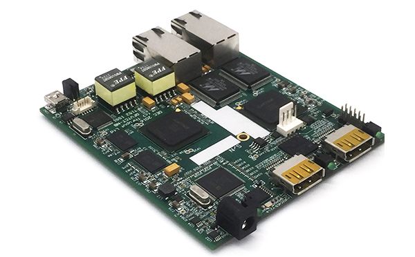
5. In the power supply layout, try to make the device layout convenient for the wiring direction of the power line. The layout needs to consider reducing the area of the input power loop. To meet the flow of the case, avoid the input power line full board running, loop area is too large. The position of power cables and ground cables is well coordinated to reduce the impact of electromagnetic interference. If the power cable and ground cable are not properly matched, many loops may occur and noise may be generated.
6, high and low frequency circuit due to different frequencies, its interference and interference suppression methods are not the same. Therefore, in the component layout, the digital circuit, analog circuit and power circuit should be separated by module layout. The high frequency circuit and the low frequency circuit are effectively isolated, or divided into small sub-circuit module board, connected with connectors.
7, layout should also pay special attention to strong and weak signal device distribution and signal transmission direction path and other issues. In order to minimize the interference, after the analog and digital circuits are separated, the high, medium and low speed logic circuits are kept in different areas on the PCB. The PCB board is partitioned according to the frequency and current switching characteristics. The noisy element is farther away from the non-noisy element. The distance between the thermal element and the heating element is longer. Low level signal channels are far away from high level signal channels and unfiltered power lines. Separate low level analog and digital circuits to avoid common impedance coupling between analog, digital and power supply common circuits.
PCB wiring
When the schematic netsheet is imported into the PCB design software, all the pins connecting the components to each other are connected through the "mouse wire", which has no network attribute significance.
This requires the engineer to connect them to each other according to the corresponding design constraints. Only when all networks are connected together do they have electrical properties. Wiring is the function of connecting all signal networks, power networks, and ground networks.
Design constraint rules should be used in PCB wiring, which include the line width of signal network, line spacing within difference, iso-length error between difference pairs, spacing requirements between transmission lines, total length of transmission lines, and requirements of segment iso-length within or between transmission lines.
After completing the layout and wiring according to the corresponding requirements, a well-proportioned PCB layout is obtained.
After PCB design is completed, production documents can be output according to production requirements, which generally include PCB production documents, PCBA production documents, steel mesh documents and so on.
PCB design inspection
Before the PCB production file is generated, the PCB design is checked in detail, including DFM, SI, PI, EMC, Thermal, and reliability. How do you check? Some companies are inspected by tools, some companies are inspected by engineers themselves, no matter which kind of, in fact, are in accordance with certain rules for inspection and analysis, that is, we usually say PCB design inspection.


