
Professional PCB manufacturing and assembly
Building 6, Zone 3, Yuekang Road,Bao'an District, Shenzhen, China
+86-13410863085Mon.-Sat.08:00-20:00


PCB(printed circuit board) is printed circuit board, referred to as printed board, is one of the important components of the electronic industry. Almost every electronic device, from electronic watches and calculators to large computers, communication electronics and military weapon systems, where there are electronic components such as integrated circuits, uses printed boards in order to make the electrical interconnection between the components. The printed circuit board is composed of an insulating base plate, connecting wires and a welding pad for assembling welded electronic components. It has the dual functions of conductive circuit and insulating base plate. It can replace the complex wiring, realize the electrical connection between the components in the circuit, not only simplifies the assembly of electronic products, welding work, reduce the traditional way of wiring workload, greatly reduce the labor intensity of workers; And reduce the volume of the machine, reduce the cost of products, improve the quality and reliability of electronic equipment. Printed circuit board has good product consistency, it can adopt standardized design, conducive to the realization of mechanization and automation in the production process. At the same time, the whole printed circuit board can be used as an independent spare part, which is convenient for the exchange and maintenance of the whole machine products. At present, printed circuit board has been widely used in the manufacture of electronic products.
The earliest use of printed circuit boards is paper-based copper-coated printed boards. Demand for printed boards has risen dramatically since the advent of semiconductor transistors in the 1950s. Especially with the rapid development and wide application of integrated circuit, the volume of electronic equipment is getting smaller and smaller, and the density and difficulty of circuit wiring are getting bigger and bigger, which requires the printed board to be updated constantly. At present, the variety of printed board has developed from single panel to double panel, multilayer and flexible board; The structure and quality have been developed to the degree of ultra-high density, miniaturization and high reliability. New design methods, design supplies and board - making materials, board - making technology continue to emerge. In recent years, a variety of computer aided design (CAD) printed circuit board applications have been popularized and promoted in the industry, in specialized printed board manufacturers, mechanized, automated production has completely replaced manual operation.

The reason why PCB can be used more and more widely is that it has many unique advantages, roughly as follows:
declassification
Over the years, the high density of printed boards has been able to develop correspondingly with the improvement of integrated circuits and the advancement of installation technology.
High reliability
Through a series of inspection, testing and aging test and other technical means, can ensure the long-term (generally 20 years of service life) PCB and reliable work.
Designability
The requirements of various properties of PCB (electrical, physical, chemical, mechanical, etc.) can be realized through design standardization, standardization, etc. This design time is short, high efficiency.
educability
PCB adopts modern management, can achieve standardization, scale (quantity), automatic production, so as to ensure the consistency of product quality.
Testability
A relatively complete test method and test standard have been established, which can be used to test and identify the qualification and service life of PCB products through various test equipment and instruments.
Assemblability
PCB products not only facilitate standardized assembly of various components, but also can be automated, large-scale batch production. In addition, the PCB and other components for integral assembly, but also can form a larger part, system, until the whole machine.
Maintainability
Because PCB products and components are assembled in a standardized design and scale production, these components are also standardized. Therefore, once the system fails, it can be replaced quickly, conveniently and flexibly, and the system can be restored quickly.
PCB also has some other advantages, such as system miniaturization, lightweight, high-speed signal transmission and so on.
The PCB was created by Austrian Paul Eisler, who first used printed circuit boards in radio in 1936. In 1943, the technology was widely used in the United States for military radios, and in 1948, the United States officially approved the invention for commercial use. Printed circuit boards have only been in widespread use since the mid-1950s. Printed circuit boards are found in almost every kind of electronic device. If there are electronic parts in a device, they are all mounted on PCBS of different sizes. The main function of PCB is to make a variety of electronic components form a predetermined circuit connection, plays the role of relay transmission, is the key electronic interconnection of electronic products, known as the "mother of electronic products".
② The core components of each functional circuit as the center, around it to carry out the layout. Components should be evenly, neatly and compactly enfolded on the PCB to minimize and shorten the leads and connections between components.
③ The circuit working at high frequency should consider the distribution parameters between the components. General circuits should be arranged as parallel as possible. In this way, not only beautiful, but also easy to assemble welding, easy to mass production.
(4) Components located at the edge of the circuit board are generally not less than 2 mm away from the edge of the circuit board. The best shape for a circuit board is a rectangle. The length to width ratio is 3:2 or 4:3. ✖ circuit board face size greater than 200 mm, 150 mm, the circuit board by mechanical strength should be considered.
Its principles are as follows:
① The wires used at the input and output ends should be avoided as far as possible. It is better to add ground wire to avoid feedback coupling.
② The minimum width of the printed board wire is mainly determined by the adhesion strength between the wire and the insulating substrate and the current value flowing through them.
When the thickness of copper foil is 0.05mm and the width is 1-15 mm, the temperature will not be higher than 3℃ through the current of 2 A, so the wire width of 1.5 mm can meet the requirements. For integrated circuits, especially digital circuits, usually choose 0.02 ~ 0.3mm wire width. Of course, whenever you can, use wide wires, especially power cables and ground cables.
The minimum distance between wires is mainly determined by the insulation resistance and breakdown voltage between wires in the worst case. For integrated circuits, especially digital circuits, as long as the process allows, the spacing can be as small as 5 ~ 8 um.
(3) The bend of the printed wire is generally a circular arc, and the right Angle or included Angle will affect the electrical performance in the high-frequency circuit. In addition, try to avoid using a large area of copper foil, otherwise, when heated for a long time, it is easy to occur copper foil expansion and shedding phenomenon. When a large area of copper foil must be used, it is best to use a grid, which is conducive to the exclusion of volatile gases generated by the heat of the adhesive between the copper foil and the substrate.
The center hole of the pad should be slightly larger than the diameter of the device lead. Too large pad is easy to form virtual welding. The outer diameter D of the pad is generally not less than d+ 1.2mm, where d is the lead aperture. For high density digital circuit, the minimum diameter of the pad is d+ 1.0mm.
According to the upstream and downstream of the industrial chain, it can be divided into raw materials, copper clad plates, printed circuit boards, electronic product applications, etc., and the relationship is simple as follows:
Glass fiber cloth: Glass fiber cloth is one of the raw materials of copper clad plate, made of glass fiber yarn textile, accounting for about 40% of the cost of copper clad plate (thick plate) or 25% (sheet). Glass fiber yarn is calcined into liquid by silica sand and other raw materials in the kiln. It is drawn into very fine glass fiber through a very fine alloy nozzle. Then hundreds of glass fiber are twisted into glass fiber yarn. Kiln construction investment is huge, generally need hundreds of millions of funds, and once the ignition must be 24 hours uninterrupted production, the cost of entry and exit is huge.
Copper foil: Copper foil is the raw material accounting for the largest proportion of the cost of copper clad plate, accounting for about 30% (thick plate) or 50% (sheet) of the cost of copper clad plate, so the price rise of copper is the main driving force of the price rise of copper clad plate.
Copper clad plate: Copper clad plate is the product of glass fiber cloth and copper foil pressed together by epoxy resin and other fusion agents. It is the direct raw material of printed circuit board. It is made into printed circuit board after etching, electroplating and laminate pressing.

Material characteristics of high frequency board
Jan 15,2023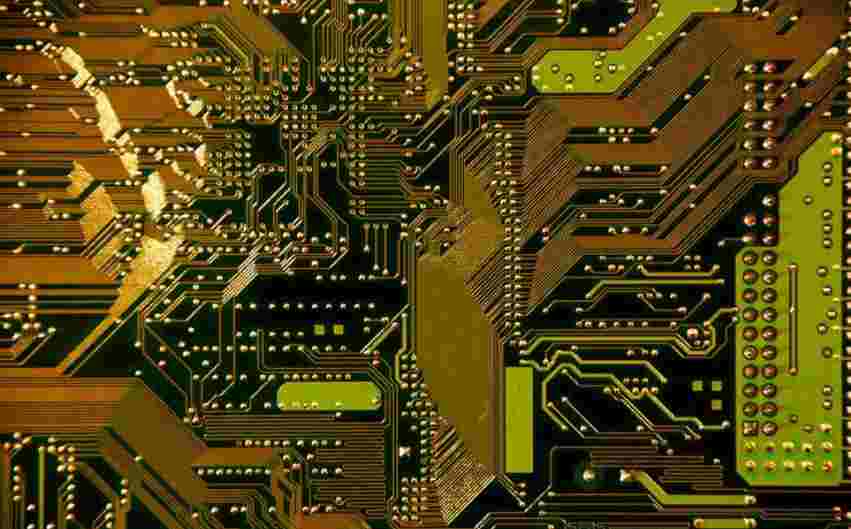


Just upload Gerber files, BOM files and design files, and the KINGFORD team will provide a complete quotation within 24h.