
Professional PCB manufacturing and assembly
Building 6, Zone 3, Yuekang Road,Bao'an District, Shenzhen, China
+86-13410863085Mon.-Sat.08:00-20:00


The top and bottom layers of the PCB's two most basic layers are copper, with a non-conductive glass fiber in the middle. Four layers of board is to use a layer of half pre-sheet to combine the two two layers of board, and so on six layers of board is three two layers of board, eight layers of board is four two layers of board.
Laminated design, two-layer board is not required, four-layer board occasionally use laminated design. The multilayer board will need to be layered design, design its each layer is what.
Copperplate surface to be covered with a layer of paint, can be called welding resistance layer. Its function is to protect the circuit board from being oxidized by the air, in addition, it can prevent the place that does not need soldering from soldering, and isolate the welding plate.
There is a silk-screen layer above the solder stop layer, which is printed with a position number. The bit number is the location of the component to facilitate welding of the component. When the design needs to place the resistance component of a specific parameter in the specified position of the line, it needs to number the location, such as R1. Usually, the character bit number on PCB is mainly resistance and capacitance, R represents resistance, and the following number represents components. C stands for capacitance, and the numbers after that are also components.

In the same type of board, the same digit character can only appear once, and each digit has its own fixed position. When there are two same bit numbers in a PCB, especially when the resistance value is different, it is easy to paste wrong when SMT is put on the machine.
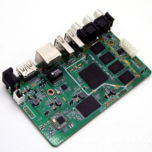
The circuit board is mainly composed of welding pad, through hole, mounting hole, wire, components, connectors, filling, electrical boundary and so on. Common board Layer structure includes Single Layer PCB, Double Layer PCB and Multi Layer PCB. The main functions of each component are as follows:
Pad: Metal hole for welding the pin of a component.
Through holes: there are metal through holes and non-metal through holes, wherein metal through holes are used to connect the pins of components between each layer.
Mounting hole: used to secure the circuit board.
Wire: Electrical network copper film used to connect the pins of a component.
Connector: A component used to connect circuit boards.
Filling: Copper applied to ground wire network can effectively reduce impedance.
Electrical boundary: Used to determine the size of the circuit board. All components on the circuit board must not exceed this boundary.
Components on PCB.
Resistor, in the circuit can be shunt, current limiting, voltage division, bias, etc.
Capacitor, two conductors close to each other, sandwiched between a layer of non-conductive insulating medium, constituting a capacitor. In a circuit, a capacitor is a device capable of storing charge.
Inductors, similar in structure to transformers, convert electrical energy into magnetic energy and store it in a circuit.
Crystal diode, which belongs to semiconductor devices, has nonlinear voltammetry characteristics, the main role is one-way conduction.
Transistor, a semiconductor device that controls current, is the core element in a circuit and can control large changes in collector current with small changes in base current.
Field effect transistor, which is a voltage controlled semiconductor device, it has a large input resistance, can be used for amplification, variable resistance, electronic switching, etc.
Two factors determine the placement of components. The first is the connection between the front and rear plates, and the second is the direction of the signal.
The basic design process of a circuit board can be divided into the following four steps:
1. Design of circuit schematic diagram
Circuit schematic design is mainly to use the schematic editor of Protel DXP to draw schematic diagram.
2: Generates a network report
The network report is the report showing the link between the circuit principle and each component, it is the bridge and link connecting the circuit diagram design and circuit board design, through the network report of the circuit diagram, you can quickly find the connection between the components, so as to provide convenience for the later PCB design.
3: the design of printed circuit board
The design of printed circuit board is usually referred to as PCB design, which is the final form of circuit schematic transformation. The related design of this part is more difficult than that of circuit schematic design. We can use the powerful design function of Protel DXP to complete the design of this part.
4: Generates a printed circuit board report
After the design of the printed circuit board is completed, various reports need to be generated, such as the generation of pin report, circuit board information report, network state report, and finally printed circuit diagram
Characteristics of circuit board
Jan 15,2023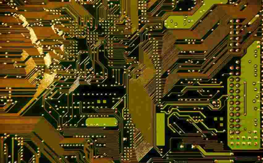


Just upload Gerber files, BOM files and design files, and the KINGFORD team will provide a complete quotation within 24h.