
Professional PCB manufacturing and assembly
Building 6, Zone 3, Yuekang Road,Bao'an District, Shenzhen, China
+86-13410863085Mon.-Sat.08:00-20:00

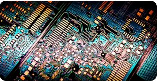
People who have been exposed to PCB production, sales and other related industries should be familiar with OSP. What does OSP mean? What are the technical points, advantages and disadvantages of PCB board OSP process flow and OSP in circuit board production? Let's briefly understand
OSP is the abbreviation of Organic Solderability Preservatives, which is translated into organic solder mask, also known as copper protector, or Preflux in English. To put it simply, OSP is to grow an organic film on the clean bare copper surface by chemical method. This film has oxidation resistance, heat shock resistance, and moisture resistance to protect the copper surface from further rusting (oxidation or vulcanization, etc.) in the normal environment; However, in the subsequent high welding temperature, this protective film must be easily removed by the flux, so that the exposed clean copper surface can be immediately combined with the molten solder to form a solid solder joint in a very short time.
In fact, OSP is not a new technology. In fact, it has been more than 35 years, longer than SMT. OSP has many advantages, such as good flatness, no IMC formation between copper and bonding pad, allowing direct welding of solder and copper during welding (good wettability), low temperature processing technology, low cost (lower than HASL), less energy use during PCB processing, etc. OSP technology was very popular in Japan in the early days. About 40% of single panels used this technology, while nearly 30% of double-sided panels used it. In the United States, OSP technology has also increased dramatically since 1997, from about 10% before 1997 to 35% in 1999.
OSP has three categories of materials: Rosin, Active Resin and Azole. At present, oxazole OSP is the most widely used. The oxazole OSP has been improved by about 5 generations, which are called BTA, IA, BIA, SBA and the latest APA respectively.
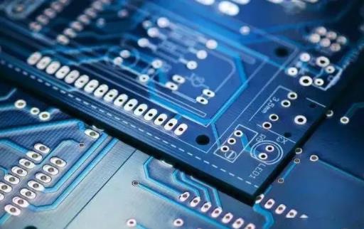
Process flow of PCB OSP:
Degreasing -->secondary water washing -->micro etching -->secondary water washing -->pickling -->DI water washing -->film forming air drying -->DI water washing -->drying
1. Degreasing
The degreasing effect directly affects the film quality. If the oil removal is poor, the film thickness is uneven. On the one hand, the concentration can be controlled within the process range by analyzing the solution. On the other hand, always check whether the oil removal effect is good. If the oil removal effect is not good, replace the oil removal fluid in time.
2. Micro etch
The purpose of micro etching is to form a rough copper surface for easy film formation. The thickness of micro etching directly affects the film formation rate. Therefore, to form a stable film thickness, it is very important to maintain the stability of the micro etching thickness. Generally, it is appropriate to control the thickness of micro etching at 1.0-1.5um. Before each shift of production, the micro etching rate can be measured, and the micro etching time can be determined according to the micro etching rate.
3. Film-forming
DI water should be used for washing before film forming to prevent the film forming solution from being polluted. DI water should also be used for washing after film formation, and the PH value should be controlled between 4.0-7.0 to prevent the film from being polluted and damaged. The key of the OSP process is to control the thickness of the anti oxidation film. The film is too thin and has poor thermal shock resistance. During reflow soldering, the film cannot withstand high temperature (190-200 ° C), which ultimately affects the welding performance. On the electronic assembly line, the film cannot be well dissolved by the flux, which affects the welding performance. Generally, it is appropriate to control the film thickness between 0.2-0.5um.
Disadvantages of PCB OSP process
Of course, OSP also has its shortcomings. For example, there are many kinds of actual formulas and different performances. That is to say, the certification and selection of suppliers should be done well enough.
The disadvantage of the OSP process is that the protective film formed is extremely thin, easy to scratch (or scratch), and must be carefully operated and released.
At the same time, the OSP film (referring to the OSP film on the unwelded connecting plate) after multiple high-temperature welding processes will change color or crack, affecting the weldability and reliability.
The solder paste printing process should be well mastered, because the poorly printed boards cannot be cleaned with IPA, which will damage the OSP layer.
The thickness of transparent and non-metallic OSP layers is not easy to measure, and the degree of transparency to coating coverage is not easy to see, so it is difficult to assess the quality stability of suppliers in these aspects;
OSP technology has no IMC isolation of other materials between Cu of PCB pad and Sn of solder. In lead-free technology, SnCu in solder joints with high Sn content grows rapidly, affecting the reliability of PCB solder joints.


Just upload Gerber files, BOM files and design files, and the KINGFORD team will provide a complete quotation within 24h.