
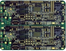
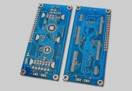
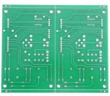
Professional PCB manufacturing and assembly
Building 6, Zone 3, Yuekang Road,Bao'an District, Shenzhen, China
+86-13410863085Mon.-Sat.08:00-20:00

Have you known what the EMI of pcb circuit board is? What are the principles of pci circuit board emi design specification?
1. Power supply processing of IC
1.1) Ensure that each IC's power PIN has a 0.1UF decoupling capacitor. For BGA CHIP, 8 capacitors of 0.1UF and 0.01UF are required at the four corners of BGA. For the power supply of PCB wiring, pay special attention to adding filter capacitors, such as VTT. This has an impact not only on stability, but also on EMI.
2. Clock line processing
2.1) It is recommended to take the clock line first.
2.2) For clock lines with a frequency greater than or equal to 66M, the number of vias per line shall not exceed 2, and the average number shall not exceed 1.5.
2.3) For clock lines with frequency less than 66M, the number of vias per line shall not exceed 3, and the average number shall not exceed 2.5
2.4) For clock lines with a length of more than 12inch, if the frequency is greater than 20M, the number of vias shall not exceed 2.
2.5) If the clock line has a via, add a bypass capacitor between the second layer (stratum) and the third layer (power layer) at the adjacent position of the via to ensure that the high-frequency current loop of the reference layer (adjacent layer) is continuous after the clock line is changed. The power layer where the bypass capacitor is located must be the power layer through which the vias pass and as close to the vias as possible. The maximum distance between the bypass capacitor and the vias shall not exceed 300 MIL.
2.6) In principle, all clock lines shall not cross the island. Here are four cases of island crossing.
2.6.1) Cross island occurs between power island and power island. At this time, the clock cable is routed on the back PCB of the fourth layer. The third layer (power layer) has two power islands, and the PCB routing of the fourth layer must cross these two islands.
2.6.2) Cross island occurs between power island and ground island. At this time, the clock cable is routed on the back PCB of the fourth layer. There is a ground island in the middle of a power island of the third layer (power layer), and the PCB routing of the fourth layer must cross these two islands.
2.6.3) Island crossing occurs between ground island and stratum. At this time, the clock line is routed on the first layer of PCB, and there is a ground island in the middle of the second layer (stratum), and the routing of the first layer of PCB must cross the ground island, which is equivalent to that the ground wire is interrupted.
2.6.4) No copper is laid under the clock line. If the conditions are limited, the clock line with a frequency greater than or equal to 66M cannot cross the island. If the clock line with a frequency less than 66M crosses the island, a decoupling capacitor must be added to form an image path. Place a 0.1UF capacitor between the two power islands and close to the cross island clock line.
2.7) When there is a choice between two vias and one island crossing, one island crossing is selected.
2.8) The clock cable shall be more than 500 MIL away from the I/O side board edge, and shall not walk with the I/O cable. If it cannot be done, the distance between the clock cable and the I/O port cable shall be more than 50 MIL.
2.9) When the clock line is running on the fourth layer, the reference layer (power plane) of the clock line should be as far as possible on the power plane that supplies power to the clock. The fewer clocks that take other power planes as reference, the better. In addition, the reference power plane of the clock line with a frequency greater than or equal to 66M must be 3.3V power plane.
2.10) The distance between clock lines shall be greater than 25 MIL.
2.11) The incoming line and outgoing line of clock line shall be as far as possible. Try to avoid similar threading methods,.
2.12) When the clock line is connected to BGA and other devices, if the clock line changes layers, try to avoid using the PCB routing form. Do not run the vias under the BGA, and preferably use the H PCB routing form.
2.13) Pay attention to all clock signals, and do not ignore any clock, including the AC of AUDIO CODEC_ Pay special attention to FS3-FS0. Although it is not a clock by name, it is actually a clock.
2.14) The pull-up and pull-down resistance of the Clock Chip shall be as close to the Clock Chip as possible.
3. I/O port processing
3.1) Each I/O port, including PS/2, USB, LPT, COM, SPEAK OUT and GAME, is divided into one piece of ground, the leftmost and rightmost are connected to the digital ground, and the width is not less than 200MIL or three vias, and other places are not connected to the digital ground.
3.2) If COM2 port is pin type, it shall be as close to I/O ground as possible.
3.3) I/O circuit EMI device shall be close to I/O SHIELD as far as possible.
3.4) The power supply layer and the stratum at the I/O port shall be separated into islands, and the Bottom and TOP layers shall be paved, and the signal shall not cross the island (the signal wire shall be pulled out of PORT directly, and the long-distance PCB wiring in the I/O PORT is not allowed). The reference of I/O port processing is given.
4. Notes
A. PCB design engineers shall strictly abide by the EMI PCB design specifications. EMI engineers have the right to inspect. PCB design engineers shall be responsible for the EMI test failure caused by violating the EMI PCB design specifications.
B. The EMI engineer is responsible for the PCB design specification and strictly abides by the EMI PCB design specification, but still fails the EMI test. The EMI engineer is responsible for providing solutions and summarizing them in the EMI PCB design specification.
C. The EMI engineer shall be responsible for the EMI test of each peripheral port, and shall not miss the test.
D. Each PCB design engineer has the right to suggest and question the PCB design specification. The EMI engineer is responsible for answering questions, and adding PCB design specifications after confirming the engineer's suggestions through experiments.
E. EMI engineers are responsible for reducing the cost of the EMI PCB design and reducing the number of magnetic beads used.


Just upload Gerber files, BOM files and design files, and the KINGFORD team will provide a complete quotation within 24h.