
Professional PCB manufacturing and assembly
Building 6, Zone 3, Yuekang Road,Bao'an District, Shenzhen, China
+86-13410863085Mon.-Sat.08:00-20:00

Explain the application of IPC through-hole standard in PCB design
I was lucky to assemble the through-hole assembly on the PCB and weld it, although there may be some challenges to overcome. Although it is much easier than threading needle, some parameters should have accurate tolerance to prevent problems in PCBA.
Fortunately, you can rely on existing IPC through-hole standards to ensure that pad or through-hole parameters are set to the best values.
What is the IPC through-hole standard?
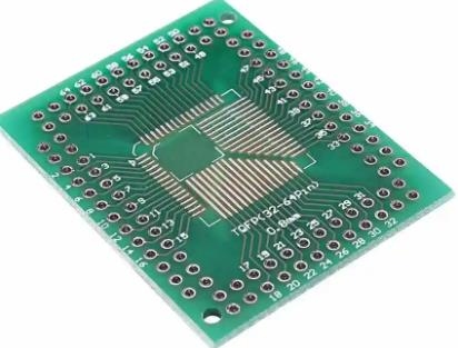
IPC through-hole standards provide guidance for landing and drilling dimensions of PTH components.
As a PCB designer, you will often encounter the term IPC. IPC was formerly known as the Institute of Printed Circuits. This is a trade organization aimed at standardizing all aspects of PCB design life cycle. You will get detailed information on how to deal with technical aspects in PCB layout, including problems with plated through-hole.
IPC-2221 and IPC-7251 have two standards, which contain guidelines for through-hole components in design. IPC-2221 is a general standard covering the electrical and manufacturing requirements of PCB boards. Section 9 of IPC-2221 specifically discusses holes and interconnections, which can provide a good reference for PTH design.
IPC-2221 provides detailed guidance on minimum ring size, pad requirements, positional tolerances, and other relevant requirements for through-hole design. The document also provides images as an example of how holes should be drilled and manufactured.
IPC-2222 is a supplement to the IPC-2222 document, which contains standards related to hard organic printed boards. IPC-2222 contains guidelines for calculating hole sizes based on density levels.
You can also find more detailed guidance in the IPC-7251 documentation. IPC-7251 is a special standard for through-hole design and pad pattern. It contains more specific criteria, such as component tolerances for various types of through hole leads, joint tolerances, and component footprint.
The parameters specified in IPC-7251 are usually specified as three levels of producibility:
Level A: general design producibility
Level B: Moderate design producibility
Level C: High design productivity
Why are IPC penetration standards important?
Ring and drill size will affect weldability.
It is a mistake to assume that through hole design is easier than surface mount design. It is easy to make irreparable mistakes in the assembly process if the regulations and standards are not followed.
For example, it is difficult to determine the drilling size of the part pad correctly. If the drill bit size is too small, you will find it difficult to insert it into the lead of the component. Pressing the assembly into a pad that is too small can damage the assembly or strip the coating.
On the other hand, spacers with drilled holes have a large tolerance, which can cause parts to become too loose after placement. This will affect solderability and PCB repair.
In addition to the size of drill bit, the size of annular ring is an important parameter in through-hole design. An annular ring is a copper area extending beyond the holes drilled on the PCB board. The ring needs to observe a minimum value. If the ring is too small, the copper around the hole is easy to fall off when heating or bearing mechanical stress during maintenance.
Calculate pad size using IPC through-hole standard
Use IPC-2221 pad size recommendations to obtain the correct pad size.
You need to determine the size of the pad to avoid the problems we have discussed. Fortunately, IPC-2221 clearly illustrates how pad sizes should be calculated. Use the following formula to obtain the correct pad size for the through-hole assembly:
Minimum pad size=maximum lead diameter+(2 x minimum ring requirements)+standard manufacturing allowance
The maximum lead diameter can be obtained from the data sheet of the component, while the other two parameters can be obtained from the corresponding table of IPC-2221 standard.
After calculating the pad size, you need to configure it in the powerful PCB design and analysis software. Try to use OrCAD because its friendly user interface makes it easy to set through hole parameters. It also has many other tools to help ensure that your design is successful for the first time. The PCB processing factory explained the application of IPC through-hole standard in PCB design, and relied on the existing IPC through-hole standard to ensure that the pad or through-hole parameters are set to the optimal value.


Just upload Gerber files, BOM files and design files, and the KINGFORD team will provide a complete quotation within 24h.