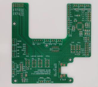
Precautions for PCB component to edge clearance in PCB design
Connecting cables, connectors, switches and other system interfaces must be available to all hands. In order to place PCB components in the best position, it is important to understand the concern of placing components too close to the edge of the board.
In this article, we will examine these potential problems and discuss some common PCB component to edge gap considerations that may be helpful.
Potential problem of insufficient PCB assembly to edge clearance
In order to obtain the best circuit board performance, the location of components must be optimized for the circuit. In general, most component placement should be more central where processors and memory chips can interconnect with their associated circuits. This will also allow these thermal devices to distribute heat evenly across the board. However, in some cases, the circuit will have to send and receive data outside the board, which will require connectors and other interface devices. These components and their associated circuits are usually located close to the edge of the circuit board.
Components that are too close to the edge of the circuit board may suffer from their placement, or in turn, may cause PCB manufacturing problems. The designer should pay attention to the following general problems:
Component location: The connector on the edge of the board must be placed correctly to interface with the cable or harness outside the board. These larger components must also be considered to avoid any interference with the airflow during the cooling process or the need for manual operation during commissioning and rework. In addition, the relevant circuits of these connectors also need to consider the requirements of edge clearance when placing components.
Circuit board assembly: Automatic PCB assembly equipment, such as pickup and play machine, wave soldering and reflow soldering furnace, all have different transportation systems for processing circuit boards. Components placed too close to the edge may interfere with the different conveyor belts used in the machine. Moreover, the higher the component near the edge of the board, the greater its potential interference to the automatic assembly process. It is better to place large parts (such as high capacitors) far away from the edge of the board.

Component damage: Circuit boards are usually produced in batches and must be removed from these panels in the future. During depanelization, the circuit board may just be bent enough to cause problems with board edge components. Solder joints may break, metal pads and marks may lift or break. Such damage may be difficult to detect and may cause intermittent circuit problems during operation. In addition, components near the edge of the board may interfere with the cutting tool used to separate the board from the panel.
Manufacturing fixtures: Circuit boards are usually placed in fixtures during manufacturing for assembly and testing. For example, in the circuit test, the circuit board is fixed in an appropriate position by vacuum decompression so that its probe firmly contacts each test point on the circuit board. This requires enough space around the edges of the circuit board to allow the test fixture to produce the air tight seal required for vacuum operation.
These are some problems that PCB layout designers should pay attention to when placing their components near the edge of the circuit board. Next, we will study some general placement rules, which will help avoid these problems.
The connector must be placed close to the edge of the circuit board, but the clearance rules must still be observed.
A rule of thumb for placing PCB components next to the edge of a circuit board
Although it is convenient to specify what components are required for plate edge clearance, the fact is that these values vary between manufacturers. However, what we can do is to lay out the different types of gaps that we should pay attention to and some general values that can be used as starting points:
Panel with V-slot: Some circuit boards can be separated from the panel by cutting the V-slot along the contour of the circuit board. In order to leave enough working space for the cutting tool without causing any damage, the component should be positioned 0.050 to 0.075 inches from the edge of the board. Higher components, such as electrolytic capacitors, should be 0.125 inches from the edge of the plate.
Panels with patch panels: Other circuit boards are wired from their panels before manufacturing and fixed in place with small patch panels until they are divided. These plates shall follow the same regular plate edge spacing as the plates to be cut, except for parts close to the splice. In these locations, the assembly should be located 0.125 inches from the lug and the higher part should have 0.250 inch clearance.
Physical support: Some circuit boards need additional support due to the overall size, thickness and weight of their components during manufacturing. To do this, brackets need to be installed on the panel and the components must not be placed where they are needed.
Copper: Although it is not a component, there should also be enough clearance between the board edges between the cabling and the power plane. This is to prevent the metal from twisting and lifting during the de panelling process. It is recommended that the copper be kept at least 0.020 inch from the edge of the plate and 0.125 inch from the tapping lugs.
Drilling: Holes are not components, but they also need to follow the board edge clearance rules. A minimum distance of 0.020 inch is recommended between the edge of the hole and the edge of the board. If the panel is to be cut from the panel using the V-groove method, the distance should be doubled.
Test point: ICT test point shall be kept 0.100 inch back from the edge of the board. This will ensure that there is sufficient space around the plate for vacuum sealing of the test fixture.
As we said, these are general recommendations for gaps. When you place components and other PCB components near the edge of the circuit board, you should pay attention to these gaps. Next we will discuss where we can get more detailed information about plate edge gaps.
The LED should be placed as close to the edge of the board as possible to improve usability.
PCB design resources that can help
You can use different resources to obtain information about PCB design, including details about the gap between components and PCB edges. The online design forum can provide help as well as technical meetings, courses and other published resources. In many cases, the company you work with already has specific design rules, as described in this article, which have been published to their engineers for use. However, the best place to obtain the design information of the circuit board being used is the manufacturer who will build the circuit board.
PCB manufacturers can tell you exactly what the physical parameters of the board are when you are still designing. They can give you the exact amount of clearance you need between components and other board objects, such as through holes, and the edges of the board. With their experience on boards that use many different types and technologies, they know what it takes to build a successful project. In addition, in addition to preparing to answer your questions, the manufacturer's engineers can also review your design to assess its manufacturability. If any DFM changes to the design are required, they will be ready to provide suggestions.
Having all this information is essential for good board design, but PCB layout engineers still need to apply all these different values when appropriate. Due to different component quantities, wiring necessity, test points and manufacturing requirements, a large amount of data needs to be tracked during layout. This is where your PCB design CAD tools can help.
The Design Rules and Constraints Manager can help you manage appropriate component gaps.
Use PCB design tools to manage correct component to board edge gaps
There are many functions inside the PCB design tool to help manage component gaps. In the figure above, you can see how to design rules and constraints specifically for component gap management in the Allegro PCB editor of Cadence. With these tools, you can set rules for nets, components, nets or groups of components, and other design objects such as drill holes, screen printing, and solder mask. Cadence's Constraint Manager also enables users to set timing constraints and other electrical rules.
Another technique that designers can use to manage the gap between components and board edges is to create a reserve around board parameters. You can set these areas for component placement and tracking routes, and you can set many of these areas as needed. By attaching rules to these areas, you can control the routing width, which layer is allowed to route, or the location of through holes and test points. Another useful function is to set a height limit in the forbidden area to prevent placing components that are too high for a specific area. The circuit board manufacturer will explain the precautions for PCB component to edge clearance in circuit board design.


