
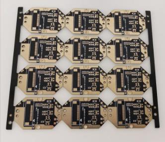
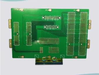
Professional PCB manufacturing and assembly
Building 6, Zone 3, Yuekang Road,Bao'an District, Shenzhen, China
+86-13410863085Mon.-Sat.08:00-20:00

What is PCB design? Now the design engineer will share with you
The design of printed circuit board is based on the circuit schematic diagram to realize the functions required by the circuit designer. The design of printed circuit board mainly refers to layout design, which needs to consider the layout of external connections. The optimal layout of internal electronic components, the optimal layout of metal wiring and through-hole, electromagnetic protection, heat dissipation and other factors. Excellent layout design can save production costs and achieve good circuit performance and heat dissipation. Simple layout design can be realized by hand, while complex layout design needs to be realized by computer aided design (CAD)
PCB design is the main function of any electronic product development process. In order to make PCB run reliably within its specification range, PCB design process is very important and must follow an effective process.
pcb design software
For large companies and self-employed PCB designers, there are many computer aided design (CAD) software packages available. The most commonly used CAD tools are Altium Designer, PAD, Allegro and OrCAD. For students and amateurs, you can use free CAD tools, such as Eagle and KiCad, although their functions are limited. The functions of PCB design software vary greatly. Basic software tools provide simpler functions, while paid tools provide more functions, such as complex cabling and simulation. With the increasing complexity and requirements of updating technology, high-end software tools are usually required.
Schematic capture
Once the design specification is completed and a clear requirements list is created for the PCB, the first step is to capture the schematic. Although schematics can be drawn manually, most schematics are captured on the computer using PCB design software. Schematic diagrams are 2D renderings that serve as blueprints for placing components and routing on PCBs. Create schematic symbols and link them to PCB pins, which define the physical dimensions of each component and the location of copper pads or through holes.
Component placement
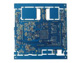
The next stage of PCB design is component placement. To integrate a component into a PCB design, all relevant information must be defined in its packaging. In addition, the size and shape of the plate, any drilling information, reservations, location of key components, etc. must be defined.
Before detailed PCB design, it is important to roughly understand the position of components on the board and determine whether there is enough space on the board to accommodate all necessary circuits. This process will also help determine how many layers are required. Once the rough placement is complete, you can begin more detailed component placement. This may take into account issues such as proximity of devices that may need to communicate with each other or may affect some signal speeds, as well as other information such as RF considerations.
route
After the placement of components, the next stage of PCB design is to route the connections (wiring) between all components. First, if the design is more complex, input a set of rules into the PCB design software. If these rules are broken, an error message will be triggered. Next, you will generate a net list from the schematic that shows all traces between all components. The critical path is completed first. In this case, the size and length of the trace are critical. Then complete the rest of the route, usually moving up and down in the layers of the PCB.
Manufacturing output
The information of PCB design photo is output in the form of Gerber file. This is the standard format used by PCB manufacturers, and is a form of NC files used by photo plotters. In addition to Gerber data, drilling information, screen printing and photoresist information will also be generated. The pick and place data is generated and used by the manufacturer to program the machine that actually fixes the components to the PCB. PCB processing and PCB assembly manufacturers explain what PCB design is? Now the design engineer will share with you.


Just upload Gerber files, BOM files and design files, and the KINGFORD team will provide a complete quotation within 24h.