
Professional PCB manufacturing and assembly
Building 6, Zone 3, Yuekang Road,Bao'an District, Shenzhen, China
+86-13410863085Mon.-Sat.08:00-20:00

The combination of rigidity and flexibility reduces the assembly cost of electronic products
Rigid flexible PCB designs can be costly to manufacture, but they can provide substantial cost savings in the assembly process of electronic systems.
In electronic products, the straight line is not always the shortest path between two points: because of the rigid flexible PCB architecture, the circuit can be folded onto itself in a 180 º bending way (stacked at the minimum height), thus reducing the size of the product.
What is a rigid flexible PCB?
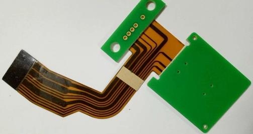
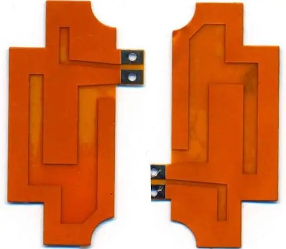
Rigid flex PCB is a combination of rigid and flexible technology. In this type of PCB, one or more flexible circuits are used to connect sub circuits in a rigid PCB. The flexible part of a rigid flexible printed circuit board is usually a multilayer circuit. The filled through holes are used to ensure the interconnection between these layers.
How can rigid flexible printed circuit boards reduce assembly costs?
The use of rigid flexible PCB in projects can save direct and indirect costs. The direct cost savings mainly come from the reduction of bill of materials and inventory. Indirect cost savings come from lower assembly costs and higher reliability.
Let's assume that a product has six interconnected rigid PCBs (power board, two control boards and three display boards). The interconnection between these boards requires harness and connector pairs. Now let's look at how using rigid flexible PCBs can reduce direct and indirect costs.
Direct cost savings
A single rigid flexible PCB with six rigid parts can be used to replace the entire assembly of six rigid PCB in the product. It also replaces the wiring harness and eliminates the requirement for connectors. Reducing inventory can directly save costs.
Indirect cost savings
Since the rigid flexible printed circuit board does not involve wiring harnesses, the cost of assembling these wiring harnesses is saved. Similarly, no harness means no wiring error, which will increase the reliability of the product. This simplifies testing procedures and reduces assembly costs.
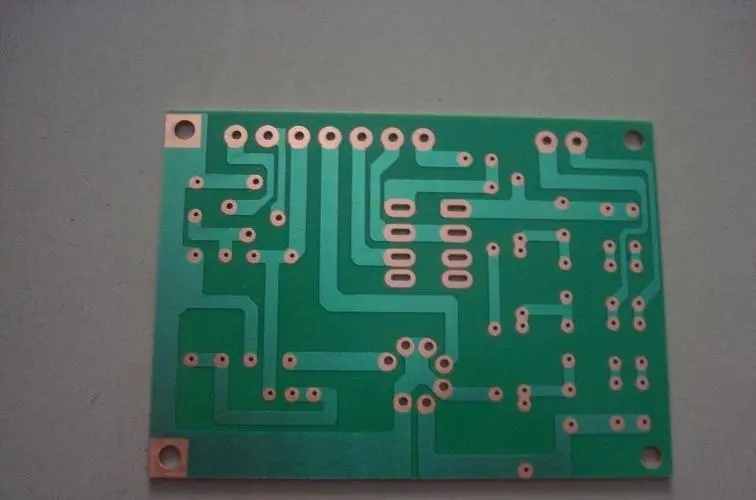
Materials used in rigid flex PCB
Rigid - Flexible PCBs use a combination of rigid and flexible materials. These materials include core material, prepreg, copper foil, flexible laminate, covering layer and bonding layer.
The thickness of the PCB material used in the flexible part is only a few microns, but it can be reliably etched. This generally makes them superior to rigid PCBs in satellite and aerospace applications.
To learn more about flexible PCBs used in satellite applications, please read our article "Flexible PCBs in satellite applications: lighter than the cloud".
The non flowing prepreg is one of the most critical components in rigid flex manufacturing. This type of prepreg can prevent the epoxy resin from flowing onto the flexible part of the PCB.
The flexible part in the rigid flexible PCB is made of an unreinforced substrate, which is made of a polyimide dielectric film coated with rolled copper. The rolled copper is more flexible than the copper foil used in rigid PCB. Therefore, the base material of the coating shall be drilled first, and then the holes shall be selectively plated. After the holes are plated, the routing and pads are etched. Bonding is used to isolate conductive layers. Bondply is a polyimide film coated with adhesive on both sides. This layer also insulates the outer surface of the flexible lamination from the ribbon extending to the rigid PCB area.
Compared with rigid materials stacked together, flexible materials have poor dimensional stability. The clearance between the hole and the copper must be at least 10 mils. The through-hole shall be placed at least 50 mils from the edge of the rigid area.
Seek guidance from manufacturers to develop your PCB stack and PCB design rules. The change in CTE (coefficient of thermal expansion) between flexible/rigid prepregs requires careful thickness balancing, especially for controlled impedance designs.
How to minimize the design cost of rigid and flexible PCB?
Keep as few layers as possible
Minimizing the number of layers can reduce the amount of prepreg required for PCB manufacturing. At the same time, fewer layers simplify the PCB manufacturing process, thus reducing the overall manufacturing cost.
Use hard laminate to achieve full thickness
In order to achieve a specific overall thickness, it is always recommended to use rigid laminates rather than other non flowing prepregs. The cost of rigid laminates is lower than that of non flowing prepregs.
Ensure that the flexible arm in the rigid flexible PCB terminates in the rigid part
If flexible PCB designers want one or more flexible arms of the flexible PCB to terminate in a flexible cable, they need additional mechanical support. This is because these flexible connections do not have the required thickness or stiffness. This leads to the cost of protecting these flexible layers during the manufacturing process. Therefore, making all flexible arms terminate at the rigid part will reduce the total cost of rigid flexible PCB design.
Design advantages of flexible part in rigid flexible PCB
The flexible part of rigid flexible PCB can take advantage of many physical design advantages, including:
360 degree bendability. This is one of the main reasons why flexible circuits are used in medical devices and wearables.
Excellent anti vibration and other destructive properties in harsh environments.
Support compact and lightweight design; The product weight can be greatly reduced.
Small flexible cables take up less space than ordinary wires.
The ability to twist or twist without any associated destruction.
To learn more about the application of flexible PCB, please read our article Why use flexible PCB in medical devices and wearable devices?
In terms of electronic product manufacturing, rigid flexible PCB also has advantages.
They provide better airflow and heat dissipation than many other PCBs.
The assembly cost is much lower than that of traditional wire harness.
Because the production process is simplified and standardized, the overall sensitivity to assembly errors is reduced, without the need to build many such harnesses, which requires cumbersome manual input.
Simplify testing procedures. The ability of rigid flexible PCB to eliminate connection problems before component assembly can prevent unnecessary waste and expense.
Flexible routing in rigid flexible PCB
The routing path in the curved area should be curved, not angled, to increase the peel strength. This recommendation is contrary to the wiring practice of rigid plates. To increase the flexibility of the ribbon, aircraft should be represented by hatches; However, cross hatches complicate impedance control. Again, careful balancing is needed. In order to improve the flexibility of the ribbon, the routing on different layers should be vertically staggered, rather than overlapping each other.
To learn more about flexible design considerations, please read our article to avoid common flexible PCB errors and successful designs.
The annular ring shall be as large as possible in the only bendable area to reduce the risk of peeling. For the same reason, the transition point from the annular ring to the routing shall be in the form of water droplets. Adding labels or anchors also helps prevent stripping.
The trace should always be perpendicular to the crease in the curved area to be bent. If the inner corners of the flexible ribbon are sharp, tear stops should be added. During the arrangement, copper can be added at the elbows of those corners for reinforcement, or polyimide reinforcement can be specified for the internal corner radius. The reinforcing layer can be laminated when the covering coating is bonded, which is the preferred method to prevent tearing. The best strategy is to avoid using sharp corners in flexible designs.
A very basic checklist for rigid and flexible design includes the following cabling considerations:
The trace shall be curved. Sharp edges along the run shall be avoided.
For rigid and flexible designs, the distance from the hole to the bend is important. That is the distance between the through hole and the rigid soft transition region. For high reliability applications, avoid less than 50 mils. Keep in mind that the rule most likely to be violated in rigid flex design is that most manufacturers do not allow the use of less than 30 mils in commercial applications.
Minimize the number of flexible layers.
Drill copper shall be 10 mils. Copper drilling is very important for rigid deflection.
Keep in mind that rigid flex PCB designs can be costly to manufacture, but can save costs during system assembly. The earlier you consult the PCB manufacturer at the planning stage, the better your PCB will be. PCB manufacturers' timely participation in the design process enables manufacturers to produce PCBs optimized for your final product. The use of rigid flexible PCB in the design will greatly reduce the assembly cost. PCB designers and PCB manufacturers explain how rigid and flexible PCB can reduce assembly costs.


Just upload Gerber files, BOM files and design files, and the KINGFORD team will provide a complete quotation within 24h.