
Professional PCB manufacturing and assembly
Building 6, Zone 3, Yuekang Road,Bao'an District, Shenzhen, China
+86-13410863085Mon.-Sat.08:00-20:00


What does the engineer explain about high-speed PCB design?
Most PCBs are considered to be at risk of some type of signal integrity problems, which are usually associated with high-speed digital design. High speed PCB design and layout focuses on creating circuit board designs that are not susceptible to signal integrity, power integrity, and EMI/EMC issues. Although no design is completely free of these problems, these problems can be reduced to an insignificant degree and will not cause performance problems in the final product.
After you create a schematic and prepare to transition to a board layout, you need to make use of specific functions in the PCB design tool for proper layout and routing. In your PCB design software, you will have the opportunity to prepare the power and grounding plane layout in the layer stack, calculate the impedance distribution of the routing, and view the stacked PCB material options. Most aspects of high-speed design revolve around PCB stack design and wiring to ensure signal and power integrity, and the correct ECAD software can help ensure success in these areas.
High speed design refers to a system that uses high-speed digital signals to transfer data between components. The dividing line between high-speed digital design and simple circuit boards with slower digital protocols is ambiguous. A general indicator for representing a particular system as "high speed" is the edge rate (or rise time) of the digital signal used in the system. Most digital designs use both high-speed (fast edge rate) and low-speed (slow edge rate) digital protocols. In today's era of embedded computing and the Internet of Things, most high-speed PCBs have RF front ends for wireless communications and networks.
Although all design starts from schematic diagram, the main part of high-speed PCB design focuses on interconnection design, PCB stack design and wiring. If you succeed in the first two areas, you are likely to succeed in the third. Read the following sections to learn how to start high-speed design and the important role of PCB design software.
Plan your PCB stack and impedance
The PCB stack you create for high-speed circuit boards will determine the impedance and ease of wiring. All PCB layers include a group of layers dedicated to high-speed signal, power supply and ground plane. The following points need to be considered when allocating layers in the layers:
Circuit board size and network number: how large the circuit board is and how many networks you need to route in the PCB layout. Physically larger boards may have enough space for you to route through the entire PCB layout without using multiple signal layers.
Wiring density: When there are many networks and the size of the circuit board is limited to a small area, you may not have enough space to wire around the surface layer. Therefore, you will need more internal signal layers when routing closer. Go to a smaller one
Number of interfaces: Sometimes, according to the width of the bus (series and parallel) and the size of the circuit board, it is a good strategy to only wire one or two interfaces on each layer. Keep all signals in the high-speed digital interface on the same layer to ensure that all signals can see consistent impedance and deflection.
Low speed and RF signals: Do you have any low speed digital or RF signals in your digital design? If so, these may take up surface space available for high-speed buses or components, and may require additional inner layers.
Power integrity: One of the cornerstones of power integrity is the use of large power layers and ground planes for each voltage level required by large ICs. These should be placed on adjacent layers to help ensure high plane capacitance to support a stable power supply through decoupling capacitors.
PCB material options, layers and thickness
Before designing your PCB stack, consider the number of layers required to accommodate all digital signals in your design. There are many methods to determine this, but these methods depend on some mathematical calculations and some past experience in high-speed circuit board design. In addition to the points of considering the number of layers listed above, large high-speed ICs with BGA/LGA footprint can determine the required circuit board size. When BGA fanout is carried out, each signal layer can normally be placed with 2 lines, and ensure that the power layer and ground layer are included in the number of layers when building the stack.
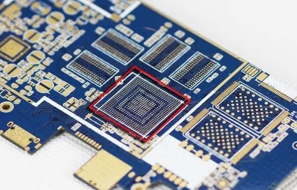
The BGA fan out on the FPGA has a large polygon for power supply in high-speed design.
FR4 grade materials can usually be used for high-speed digital design, as long as the route between components is not too long. If the route does become too long, there will be too much loss in your high-speed channel, and the components at the receiving end of the channel may not be able to recover the signal. The main material property to be considered when selecting materials is the loss tangent of PCB laminate. The channel geometry will also determine the loss, but the FR4 laminate with a lower loss tangent is usually a good place to start on a smaller circuit board.
If your line is too long, you may need more professional materials as the base material of high-speed signal. PTFE based laminate, dispersed glass laminate or other special material systems are ideal for supporting large high-speed digital boards, where the wiring is long and low insertion loss is required. A good combination of entry-level high Tg laminated materials for small high-speed PCBs is 370HR. For larger circuit boards, such as Megtron or Duroid laminates are a good choice. Before continuing, please check with your manufacturer to ensure that your material selection and recommended laminations are manufacturable.
Impedance control
The impedance can be determined only after you have created the recommended stack and verified it with your manufacturer. The manufacturer may recommend modifications to the PCB stack, such as alternative PCB material options or layer thickness. Once you have obtained permission on the layer to be used and finalized the layer thickness, you can begin to calculate the impedance value.
Impedance is usually calculated using formulas or calculators with field solver tools. The impedance required in the design will determine the size of the transmission line and the distance from the nearby power source or ground plane. The following tools can be used to determine the transmission line width:
Formulas of IPC-2141 and Waddell: These formulas provide a starting point for impedance estimation, and they produce accurate results at lower frequencies.
2D/3D field solver utility: The field solver is used to solve Maxwell equations in the transmission line geometry you define for high-speed plates.
Using the layer stack manager with the field solver will give you the most accurate results, taking into account copper roughness, etching, asymmetric line alignment, and differential pairs. After the impedance curve of the route is calculated, it needs to be set as a design rule in the routing tool to ensure that the route has the required impedance.
Impedance calculation of transmission line design in high-speed board. The layer stack manager in Altium Designer includes an impedance calculator for calculating copper roughness.
Most high-speed signal protocols (such as PCIe or Ethernet) use differential pair routing, so you need to design specific differential impedance by calculating the routing width and spacing. The field solver tool is the best tool for calculating the differential impedance of any geometry (microstrip, stripline, or coplanar). Another important result of the field solver utility is propagation delay, which is used to force length adjustments during high-speed cabling.
Layout planning for high-speed PCB
There are no specific rules or standards for where components should be placed in a high-speed PCB layout. In general, it is a good idea to place the largest CPU IC near the center of the circuit board, because it usually needs to be connected to all other components on the circuit board in some way. Smaller ICs directly connected to the central processor can be placed around the central IC so that the wiring between components can be kept short and direct. Peripheral devices can then be placed around the circuit board to provide the required functionality.
When the main controller IC is placed near the center of the circuit board and other high-speed peripherals are placed around it, the high-speed layout is the best. This is one of the reasons why the motherboard places a large processor in the center of the motherboard. The MiniPC project in Altium Designer places its PCIe, DDR4, USB 3.0 and Ethernet peripherals around the central FPGA SoC, so wiring is easier.
After placing components, you can set up design tools to help you start designing the routing. This is a sensitive part of high-speed circuit board design, because incorrect wiring will damage signal integrity. However, if the previous steps are completed correctly, signal integrity is easier to achieve. You should set the impedance curve in PCB design rules so that any wiring in the design is placed with the correct width, gap, and spacing to maintain controlled impedance during wiring.
Routing, signal integrity and power integrity
Signal integrity starts with a specific impedance value in the design circuit board and maintains that value during layout and wiring. Other strategies to ensure signal integrity include:
Designed to shorten the path between components to ensure high speed signals
Minimize wiring through vias. Ideally, only two vias are used to access the internal layer
Eliminate stubs on ultra-high speed lines (such as 10G+Ethernet) through back drilling
Note whether any terminal resistance is required to prevent signal reflection; Check the data table to see if there are on-chip terminations
Consult your manufacturer to find out which materials and processes can help you avoid fiber weaving effects
Use rough crosstalk calculations or simulations to determine the proper spacing between networks in a board layout
Keep a list of buses and networks that need to be matched in length so that you can apply an adjustment structure to eliminate skew
These important points can be coded as design rules for the routing tool, which will help ensure that you follow best practices for high-speed design.
High speed PCB wiring
The design rules you set up in a high-speed design project will ensure that you meet impedance, spacing, and length goals when designing your wiring. In addition, important rules in differential pair routing can be enforced in your routing, especially to minimize length mismatch to prevent skew and forced spacing between routes to ensure that the differential impedance target is met. The best routing tools will allow you to encode routing geometric constraints into design rules to ensure performance.
Length tuning is used across traces in parallel buses and differential pairs to ensure time delay matching and eliminate the bias between signals seen at the receiver.
One of the most important points in high-speed PCB routing is to place a ground plane near the routing. The stack shall be constructed to have a ground plane in the layer adjacent to the impedance control signal, so as to maintain consistent impedance and define a clear return path in the PCB layout. The wiring shall not pass through the gap or split of the ground plane to avoid the impedance discontinuity causing EMI problems. Ground plane placement is not only limited to ensuring signal integrity, but also plays a role in power supply integrity and ensuring stable power supply.
Power integrity
Ensuring a stable power supply to high-speed components is critical in PCB design because power integrity issues often masquerade as signal integrity issues. They also generate unnecessary radiation from interconnects and buses, because transients generate strong oscillations and strong radiation. To ensure stable power transmission, use a decoupling capacitor bank with a series of autoresonances to ensure that the design has low impedance within the widest possible bandwidth. Using power and ground plane pairs on adjacent layers provides additional capacitance to help maintain low PDN impedance.
Advanced tools for high-speed design and layout
The best high-speed PCB design software integrates all these functions into one application, rather than forcing you to use separate workflows to overcome different design challenges. High speed PCB designers must perform a lot of work on the front end to ensure signal integrity, power integrity, and electromagnetic compatibility, but the correct high-speed layout tools can help you implement results according to design rules to ensure that the design performs as expected.
More advanced PCB design software will interact with simulation applications to help you perform industry standard analysis. Some simulations are dedicated to evaluating signal integrity and power integrity in new designs, as well as checking EMI in PCB layouts. Simulations are very useful in high-speed design because they can help users identify specific SI/PI/EMI problems before putting the design into manufacturing. Some examples include returning path tracking, locating impedance discontinuities in routing, and ideal placement of decoupling capacitors to prevent EMI.
Use the best high-speed design software to complete your physical layout.
When you need to build advanced high-speed digital systems while ensuring signal integrity and power integrity, use the best high-speed design and layout toolset based on the rule driven design engine. Whether you need a board computer with dense layout or a complex mixed signal PCB, the best PCB layout tools will help you maintain flexibility when creating high-speed PCB layouts. Circuit board assembly and circuit board processing manufacturers explain what high-speed design of circuit board, high-speed PCB design and layout are.


Just upload Gerber files, BOM files and design files, and the KINGFORD team will provide a complete quotation within 24h.