
Professional PCB manufacturing and assembly
Building 6, Zone 3, Yuekang Road,Bao'an District, Shenzhen, China
+86-13410863085Mon.-Sat.08:00-20:00

Basic knowledge of power integrity in PCB layout
For many years, PCB layout engineers have dealt with power and grounding in this way - as long as the circuit board has VCC and ground plane, just put vias into it to get a continuous power supply. However, for today's high-speed design, the facts are quite different.
The power supply in the circuit board may not be a calm and picturesque lake, but a nightmare like a storm, full of ripples and waves threatening to submerge the boat. Components required for high-speed circuits require a large amount of power, which will generate spike signals, threatening the smooth operation of other components on the circuit board. For the best performance of the circuit board, the integrity of this water must be managed so that the circuit board can provide a balanced and continuous power supply for all its needs. The following are some power integrity basics that can help you calm the power supply network storm in your design.
Circuit board problems due to power integrity defects
Once upon a time, circuit board components were very simple. Many components had only one power supply and one grounding pin. These devices are very easy to use, especially through hole versions, because they can be easily connected to the VCC and ground plane of the circuit board. Even their bypass capacitors are easy to place and wire because they are just on the top of the part and can be easily wired to pin 14 of the IC. In addition, these components are not so sensitive to small fluctuations in the power supply network, and their signal speed is not fast enough to cause problems. However, with the components used in today's high-speed design, all of this has changed dramatically.
The power supply network (PDN) of the circuit board must be carefully managed to provide clean power to all its components through the PCB. Circuit boards that are not designed for good power integrity may have many problems, such as crosstalk power ripple in high-speed circuits of circuit boards. We will further study different types of problems that poor power integrity may bring to the circuit board. But first, let's look at the results of these problems:
Excessive noise in the PDN will affect the required voltage level of the components. If they are below an acceptable level, the relevant circuit may fail.
Even if the voltage is within the tolerance range required by the device, the noise on the PDN may also be shown as crosstalk on the signal, resulting in misunderstanding of these signals.
PDN noise may radiate EMI through the plane and connection of the power supply network.
All of the above situations will bring great trouble to designers during testing and debugging.
Obviously, good power integrity in PCB design is critical to the success of the design. Therefore, let's explore some basic knowledge of power integrity.
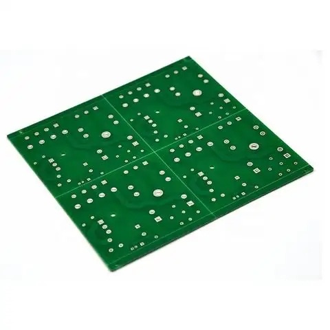
The layout of these components facilitates short and direct cabling, which contributes to power integrity
Noteworthy power integrity basis
Good power integrity in a circuit board means that its power transmission network is designed to provide a stable voltage reference and distribute power to all circuit board components within acceptable noise and tolerance. The PDN must be able to evenly distribute power throughout the system - from the power supply to the associated wiring and vias, through the plane and capacitors, and finally to individual devices. Each device on the board needs to be strictly controlled and supplied with consistent voltage to ensure consistent and stable operation. Some of these devices, such as large pin count processors, require several different voltages and higher currents than other components to operate. The requirements of these components must be managed by the PDN, otherwise it will adversely affect other components on the circuit board. PCB assembly and PCB processing manufacturers explain the basic knowledge analysis of power integrity in PCB layout.
Ground bounce
With the increase of switching speed in high-speed design, the low level state of the signal may not always return to the reference ground level. This ground bounce is also known as synchronous switching noise or SSN. As the low level of the signal drifts upward, it may eventually be misunderstood as the high level, resulting in incorrect data transmission.
Power ripple
The switching of SMPS (switching mode power supply) will cause the power ripple to spread throughout the design. These ripples may cause crosstalk, overwhelm and interfere with the operation of nearby circuits.
electromagnetic interference
If the design is incorrect, switching SMPS between switch states will generate EMI. EMI will not only affect the smooth operation of on-board circuits, but also interfere with external electronic devices. EMI is also closely related to the configuration of the power supply and ground plane of the circuit board. These planes not only provide power and ground for the PDN, but also serve as effective EMI shielding. Shielding must also be considered in the plane configuration.
Signal return path
Although a clear signal return path is part of creating good signal integrity, the reference plane is part of the circuit board PDN system and must be considered when designing power integrity. High density components will have many vias for signal and power and ground connections, but these vias will block the clear return path on the reference plane. In addition, some power requirements may cause the designer to split the plane. However, these splits may affect the clear return path of high-speed signals - generating more EMI - and must be carefully designed.
Now that we have seen some basic power integrity issues, let's look at PCB layout best practices and power integrity basics that can help prevent these issues.
PCB distribution
PCB Layout Skills for Good Power Integrity
In PCB layout design, the following are some areas that require close attention to avoid some power integrity issues that we have been discussing.
Layered stacking configuration
The PDN of a circuit board is closely related to the layer configuration in the circuit board stack. The ground plane must be strategically placed to provide microstrip and stripline layer configurations for sensitive signal routing. These layers will provide the required clear signal return path and provide EMI shielding. It is also important to lay out the floor plan to ensure that all power is delivered to each component. This may require splitting the power layer for different voltages. By first formulating the design plan, you will better understand the different functional partitions and configure your PDN accordingly.
Component placement
The reference voltage must be carefully managed in the PDN to ensure that the components receive the required power. This will prevent the false triggering of sensitive signals caused by ground bombs. This means adding multiple bypass capacitors to stabilize the PDN to meet the needs of processors and other power consuming components. You need to place these capacitors as close as possible to the power supply pins to which they are connected. It is also important for the power supply to place components together on the same side of the circuit board like this, because short and direct wiring is essential. Remember to keep analog, digital and power parts of the circuit isolated from each other to prevent power noise from interfering with analog and digital signals.
Trace Route
The wiring from the power supply pin to the bypass capacitor should be as short as possible. When wiring the power supply, use a 45 degree angle or fillet to make these wires as short, wide and straight as possible. Wider routing is necessary to increase the current and temperature of the power network. At the same time, it will reduce the inductance on the line and help prevent crosstalk. Shorter cabling in the PDN will also minimize the possibility of these cabling running as an antenna and generating additional noise. Remember to keep digital and analog cabling away from the power area to protect them from noise.
It is better to use a solid plane for grounding rather than routing. This will help with thermal management and power integrity, but it will also help signal integrity by providing a clear signal return path for sensitive high-speed transmission lines. But remember not to block clear signal paths with cuts, splits, or large groups of vias. When creating the ground plane, make sure that its outline contains all the components that contribute to EMI shielding. And, most importantly, remember to carefully plan the planar divisions to ensure that power is evenly distributed across all components. PCB assembly and PCB processing manufacturers explain the basic knowledge analysis of power integrity in PCB layout.
There are many functions in PCB design tools that can help create good power integrity in the design. Next, we will study how to make the best use of these functions.


Just upload Gerber files, BOM files and design files, and the KINGFORD team will provide a complete quotation within 24h.