
Professional PCB manufacturing and assembly
Building 6, Zone 3, Yuekang Road,Bao'an District, Shenzhen, China
+86-13410863085Mon.-Sat.08:00-20:00

Circuit board design, electronic hardware product prototype design
How you begin to prototype the electronic components of the product depends on the questions you want to answer. Each time you create a new prototype, you should have clearly defined questions that the prototype should answer. If you have broad questions about whether your product will work, or whether it will solve the expected problems, you should have started using prototypes based on earlier similar works of the development suite (such as Arduino or Raspberry Pi).
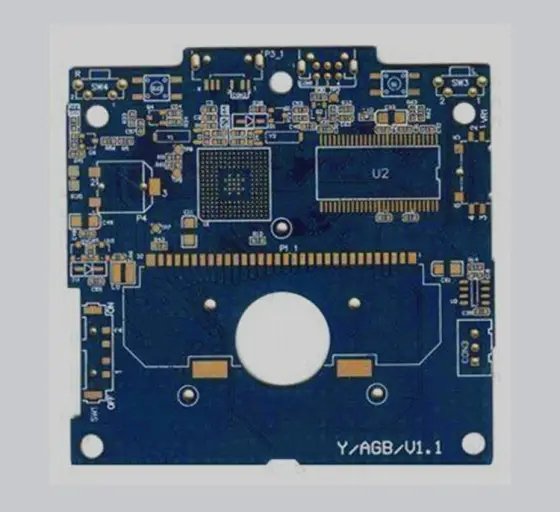
If there is no major problem with your product functions, you may want to design custom PCBs directly. Most large companies that develop products begin with customized PCBs. This is the fastest way to market, although it may not be the cheapest. The prototype design of customized PCB includes two steps: producing bare PCB and welding all components. We will discuss each process separately.
Although there are PCB technologies for home production, they are limited to simple design. Therefore, you may need to outsource PCB prototype production. Assuming that you do not manufacture and assemble your own PCB, you will use the same process to produce prototype boards and mass produce your boards.
PCB production can be summarized into the following steps:
The process starts with a laminated core made of woven glass epoxy resin. It is used as an insulator between conductive layers and provides physical strength for circuit boards.
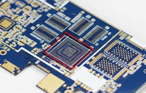
The single panel consists of a laminated core and a copper layer on one side. The double-sided panel consists of a laminated core with copper layers on each side. The multilayer board is composed of alternating copper layers and laminated core layers. Most boards will use two, four, six, or eight conductive layers.
The layout design of each conductive copper layer is drawn on the film by laser, and photosensitive chemical "resist" is applied. The copper layer is then exposed to high intensity ultraviolet light penetrating the film. This light hardens any copper traces and the resist layer on the pad.
The copper layer is then treated with a chemical solution to remove any resist layer that is not hardened by ultraviolet light. This leaves only the hardened corrosion inhibitor material on the required copper traces and pads. Any exposed copper not covered by the resist is then removed with another chemical. The hardened resist layer is then removed, leaving only the copper needed to form traces and pads.
Next, all layers are bonded together to form stacked PCBs using a laminating process.
Drill holes on the PCB stack to form through holes for connecting signals on different layers. Any holes in the through hole assembly are also drilled. However, it is usually best to use only surface mount technology (SMT) components to minimize welding costs.
Copper is then deposited on all exposed metal surfaces, including the inner walls of any holes. Additional copper is plated to all exposed copper surfaces.
Now that the bare PCB has been completed, the next step is to place and weld all electronic components. Robotic equipment, known as a pickup and placer, uses a vacuum system to pick up components and place them precisely on a PCB. Solder paste (a viscous mixture of solder and flux) is used to temporarily secure parts.
Finally, the circuit board melts the solder paste through the reflow furnace and forms a permanent electrical connection between components and PCB pads. The circuit board assembly and circuit board processing manufacturers explain the basic guidelines for circuit board design and prototype design of electronic hardware products.
Engineering prototype
Engineering prototype (sometimes called appearance prototype of similar works) is the first time to combine appearance and function in a prototype. Once you have an engineering prototype, you will finally have something of sufficient quality to show to customers and investors.
This is the time to seek outside investors to become more practical. By this stage, you have overcome most of the engineering and manufacturing risks. Investors clearly like this risk reduction.
For my own hardware products, I funded the product development at this stage myself. I used my prototype to make a large national retailer interested in my products. From there, I used this success to find manufacturers willing to fund the remaining prototype stages.
Engineering prototypes are close to mass production prototypes, but have not yet been tested or ready for mass production.
Pre production prototype
This is a prototype with similar appearance, which has been optimized for manufacturing. This is very close to the final product your customers will see. In most cases, if the product will be sold through retail stores, it should also include retail packaging.
Although the appearance and function of pre production prototypes may be very similar to those of similar works, the key difference is manufacturability. In the process of product development, many entrepreneurs underestimate the work required to migrate from prototypes to products that can be efficiently manufactured. Making several prototypes is quite different from making millions of units. In most cases, a large amount of additional design work is required to prepare the design for mass manufacturing.
For example, 3D printing or CNC machining is usually used when prototyping the product shell. For large-scale manufacturing, high pressure injection molding will be used to produce shells.
3D printing and CNC processing are very tolerant technologies. You can make prototypes of almost any imaginable plastic shape. This is not the case with injection molding. Injection molding has very strict production requirements. After completing the 3D printing prototype, it is necessary to further upgrade the injection molding design.
Injection molding: 3D printing is very suitable for producing dozens of parts. However, it is impractical to produce hundreds of parts. Finally, injection molding is necessary for mass production of your product shells. Not surprisingly, the injection molding process starts with the creation of molds. The mold is made of metal, and the hardness of metal determines the service life and cost of the mold.
For prototyping or early production, aluminum dies are usually the best choice. Aluminum molds typically cost thousands of dollars and can produce up to about 10000 parts. When hot molten plastic is injected into the mold under high pressure, the mold forms two halves. In order to produce fine detail in the part, high pressure is necessary. Once the plastic has cooled and cured, open the mold and remove the part.
Most designs require major modifications to prepare them for injection molding. Make sure that the person who designed your shell understands injection molding, or you may end up with a product that can be prototype but cannot be mass produced. It is a great achievement to have a prototype with complete functions, normal work and similar appearance, so once you reach this milestone, please pat yourself on the back!
But don't get too excited... The transition from prototype to mass manufacturing is one of the most underrated steps to bring new hardware products to market.
Engineering Verification Test (EVT)
Once you have completed the project prototype, you can start testing it to verify that it works exactly as specified.
The first phase of this test is called Engineering Verification Test (EVT). This testing phase focuses on electronics. Typically 10-50 units will be tested during EVT. The EVT will include testing basic functions, but also various stress tests to ensure that there are no hidden problems. This includes power, thermal, and EMI tests. The goal of EVT is to verify that your prototype meets the functional, performance, and reliability specifications.
Design Verification Test (DVT)
Design Verification Testing (DVT) is one of the most complex phases. The objective is to ensure that the product complies with any necessary appearance and environmental specifications. Compared with the EVT phase, the number of units required is much more, usually 50-200 units. These devices will be subjected to very rigorous tests, including drop, fire and water resistance tests. One of the main objectives of design verification testing is to verify whether the product is durable enough to withstand daily use. This is usually also the stage of obtaining electrical certification. This includes FCC, CE, UL and RoHS certifications. Due to the cost and time required to obtain the necessary electrical certification, the process is usually delayed to the DVT stage. This is to ensure that no other design changes are required after the certification test starts. Of course, if any problems are found during certification testing, the design may need to be modified to correct them. The circuit board assembly and circuit board processing manufacturers explain the basic guidelines for circuit board design and prototype design of electronic hardware products.


Just upload Gerber files, BOM files and design files, and the KINGFORD team will provide a complete quotation within 24h.