
Professional PCB manufacturing and assembly
Building 6, Zone 3, Yuekang Road,Bao'an District, Shenzhen, China
+86-13410863085Mon.-Sat.08:00-20:00

What impact does PCB design common pad have on PCBA processing
PCB design and PCB manufacturer introduction What impact does the PCB design common pad issue have on PCBA processing?
The design of printed circuit board is based on the circuit schematic diagram to realize the functions required by the circuit designer. The design of printed circuit board mainly refers to layout design, which needs to consider the layout of external connections. The optimal layout of internal electronic components, the optimal layout of metal wiring and through-hole, electromagnetic protection, heat dissipation and other factors. Excellent layout design can save production costs and achieve good circuit performance and heat dissipation. Simple layout design can be realized by hand, while complex layout design needs to be realized by computer aided design (CAD)
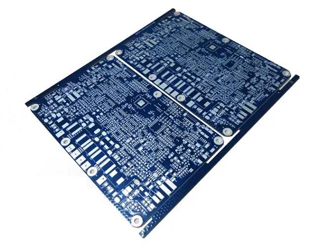
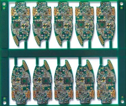
PCB is a very important thing in electronic products. The quality of an electronic product depends largely on the quality of PCB design. Next, we will introduce the impact of PCB design common pad on PCBA processing.
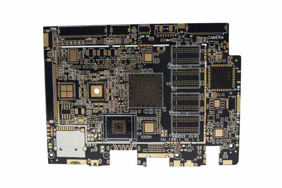
Importance of PCB pad design
PCB pad design is a very critical part of PCB design. It determines the welding position of components on PCB, and plays a significant role in the reliability of solder joints, possible welding defects during welding, clarity, testability and maintainability.
If the PCB pad design is correct, a small amount of skew during mounting can be corrected due to the self correction effect of the surface tension of molten solder during reflow soldering. On the contrary, if the PCB pad design is incorrect, even if the mounting position is very accurate, there will be component displacement, monument and other welding defects after reflow soldering. Therefore, pad design is one of the key factors to determine the manufacturability of surface mount components.
Common pad is a common and frequently occurring disease in PCB design, and it is also one of the main factors causing the hidden trouble of PCBA processing quality.
The Influence of PCB Design Common Pad on PCBA Processing
1. After the chip components are welded on the same bonding pad, if the pin plug-in components or wiring are welded again, there is a hidden danger of false soldering during secondary welding.
2. It limits the number of repairs during subsequent commissioning, testing and after-sales maintenance.
3. During maintenance, components around the same bonding pad are desoldered when a component is desoldered.
4. When the pad is shared, the stress on the pad is too large, which causes the pad to peel off during welding.
5. The components share the same bonding pad. The amount of tin is too much, and the surface tension after melting is asymmetric. The components are pulled to one side, resulting in displacement or monument.
6. Similar to the non-standard use of other pads, the main reason is that only circuit characteristics and area or space constraints are considered, resulting in a lot of component installation and solder joint defects during assembly and welding, which have a great impact on the reliability of circuit work.
The above is my introduction to "What impact does the PCB design common pad issue have on PCBA processing? The importance of PCB pad design" for your reference.


Just upload Gerber files, BOM files and design files, and the KINGFORD team will provide a complete quotation within 24h.