
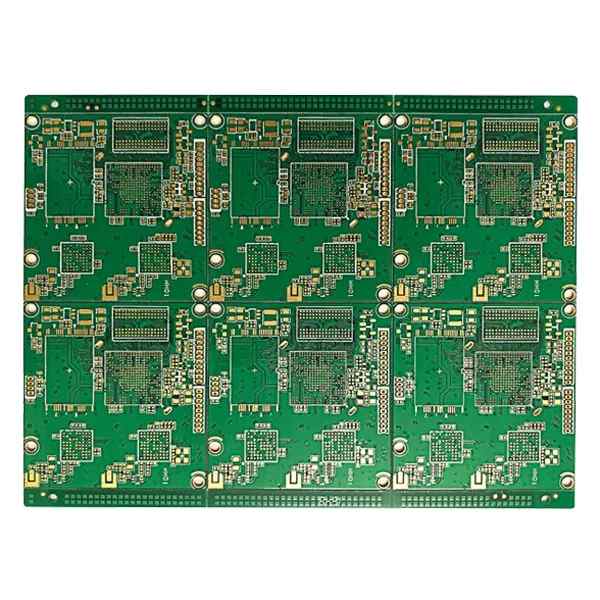
Professional PCB manufacturing and assembly
Building 6, Zone 3, Yuekang Road,Bao'an District, Shenzhen, China
+86-13410863085Mon.-Sat.08:00-20:00

PCB design: introduction to wiring skills of amplifier PCB
In the process of circuit design, application engineers often ignore the layout of printed circuit board (PCB). A common problem is that the circuit schematic is correct, but it does not work, or it can only operate under low performance. I will show you how to correctly arrange the circuit board of the operational amplifier to ensure its function, performance and robustness.
Recently, I worked with an intern to study OPA191 operational amplifier with in-phase configuration with 2V/V gain, 10k Ω load and+/- 15V supply voltage.
I asked the intern to make the layout for the design, and gave him general guidance on PCB layout (for example, try to reduce the wiring path of the circuit board, and try to keep the components arranged closely to reduce the space occupied by the circuit board), and then let him design by himself. How difficult is the design process? It's just a few resistors and capacitors, isn't it?
Seeing his first layout attempt, I realized that the layout of the circuit board was not as intuitive as I thought; I should at least give him some more detailed guidance. He followed my advice completely in design: shorten the wiring path and put the parts together tightly. However, there is still much room for improvement in this layout in order to reduce the parasitic impedance of the circuit board and optimize its performance.
The next step is to improve the layout. The first improvement we made is to move resistors R1 and R2 to the inverting pin (pin 2) of OPA191; This helps to reduce the stray capacitance of the inverting pin. The inverting pin of the operational amplifier is a high impedance node, so it has high sensitivity. The longer routing path can be used as a conductor to couple high-frequency noise into the signal chain. PCB capacitance on the inverting pin can cause stability problems. Therefore, the contacts on the sinking pins should be as small as possible.
Moving R1 and R2 to pin 2 allows the load resistor R3 to rotate 180 degrees so that decoupling capacitor C1 is closer to the positive power supply pin (pin 7) of OPA191. It is important that the decoupling capacitor be as close to the power supply pin as possible. If the wiring path between the decoupling capacitor and the power supply pin is very long, the inductance of the power supply pin will increase, thus reducing the performance.
After moving the part to a new location, you can still make some other improvements. You can widen the routing path to reduce inductance, which is equivalent to the size of pads connected by the routing path. The top and bottom ground planes of the board can also be grouted to create a reliable low impedance path for the return current.
The next time you lay out a printed circuit board, it is recommended that you follow the following layout conventions:
1. Minimize the connection of inverting pins.
2. Place the decoupling capacitor as close to the power supply pin as possible.
3. If multiple decoupling capacitors are used, place the smallest decoupling capacitor closest to the power supply pin.
4. Do not place vias between decoupling capacitors and power supply pins.
5. Expand the routing path as much as possible.
In the above, we talked about the correct layout of the instrument amplifier (op amp) PCB, and provided a series of good layout practices for reference. Next, we will discuss common mistakes when arranging the instrument amplifier (INA), and then show how to correctly arrange the INA PCB.
INA is used for applications where differential voltage amplification is required, such as measuring the voltage across shunt resistors in high-end current detection applications.
The differential voltage is measured through RSHUNT. R1, R2, C1, C2 and C3 are used to provide common mode and differential mode filtering, R3 and C4 are used to provide output filtering for U1 INA, and U2 is used to buffer INA reference pins R4 and C5 are used to form a low-pass filter to greatly reduce the noise introduced by the operational amplifier to the INA reference pin.
The first error is to measure the differential voltage Rshunt through resistance. It can be seen that the resistance of wire Rshunt to R2 is shorter than that of wire Rshunt to R1. This difference in line impedance may introduce the input bias current into the INA, resulting in a differential voltage on the U1 input side. Since the task of INA is to amplify the differential voltage, the unbalanced line on the input side may cause errors. Therefore, it is necessary to ensure that the INA input line is balanced and as short as possible.
The second error is related to the INA gain setting resistor Rgain. The length from U1 pin to Rgain pad is longer than the actual required length, so additional resistance and capacitance will be generated. Since the gain depends on the resistance between the INA gain setting pin, pin 1, and pin 8, additional resistance may result in incorrect target gain. Since the gain setting pin of the INA is connected to the feedback part of the INA, additional capacitance may cause stability problems. Therefore, make sure that the line connecting the gain setting resistor is as short as possible.
Then, it may be necessary to improve the position of the reference pin of the buffer circuit. The reference pin buffer circuit is far away from the reference pin, which may increase the resistance of the reference pin, causing noise or other signals to be coupled into the line. The additional resistance on the reference pin may reduce the high common mode rejection ratio (CMRR) provided by most INAs. Therefore, the reference pin buffer circuit should be placed as close to the INA reference pin as possible.
In Figure 7, it can be seen that R1 and R2 have the same line length to the shunt resistor, and Kelvin connection is used. The gain setting resistance of INA pin should be as short as possible, and the reference buffer circuit should be as close to the reference pin as possible.
If you want to lay out PCB for INA in the future, please follow the following guidelines:
1. Ensure that all lines at the input end are completely balanced;
2. Reduce the line length and minimize the capacitance on the gain setting pin;
3. Arrange the reference buffer circuit as close to the INA reference pin as possible;
4. The decoupling capacitor shall be arranged as close to the power supply pin as possible;
5. At least one layer of solid ground plane shall be covered;
6. Don't sacrifice good layout to use silk screen for electronic components;
7. Follow the guidelines mentioned in the first part of this article. PCB design and PCB processing manufacturers show how to correctly arrange the circuit board of operational amplifier to ensure its function, performance and robustness.


Just upload Gerber files, BOM files and design files, and the KINGFORD team will provide a complete quotation within 24h.