
Professional PCB manufacturing and assembly
Building 6, Zone 3, Yuekang Road,Bao'an District, Shenzhen, China
+86-13410863085Mon.-Sat.08:00-20:00

The design of circuit board affects PCB welding quality. In terms of layout, when the size of circuit board is too large, although the welding is easy to control, the printing line is long, the impedance increases, the anti noise ability decreases, and the cost increases; If it is too small, the heat dissipation will drop, and the welding is not easy to control, which is easy to occur
The design of circuit board affects the welding quality
In PCB layout, when the size of the circuit board is too large, although the welding is easier to control, the printing line is long, the impedance increases, the noise resistance decreases, and the cost increases; If it is too small, the heat dissipation will drop, the welding is not easy to control, and the adjacent lines will easily interfere with each other, such as the electromagnetic interference of the circuit board. Therefore, PCB design must be optimized: (1) Shorten the connection between high-frequency components and reduce EMI interference. (2) Components with large weight (such as more than 20g) shall be fixed with supports and then welded. (3) Heat dissipation shall be considered for heating elements to prevent large Δ In case of defects and rework, the thermal sensor shall be far away from the heat source. (4) The arrangement of elements shall be as parallel as possible, which is not only beautiful but also easy to weld, and it is suitable for mass production. The circuit board is designed as a 4 ∶ 3 rectangle. The wire width shall not be abrupt to avoid the discontinuity of wiring. When the circuit board is heated for a long time, the copper foil is easy to expand and fall off. Therefore, large area copper foil should be avoided.
PCB manufacturers tell you that high-quality PCB should meet the following requirements
1. The telephone shall be easy to use after the components are installed, that is, the electrical connection shall meet the requirements; The line width, line thickness and line spacing of the line shall meet the requirements to avoid heating, open circuit and short circuit of the line;
2. The copper skin is not easy to fall off under high temperature; The copper surface is not easy to be oxidized, which affects the installation speed. It will be damaged soon after being oxidized;
3. No additional electromagnetic radiation; The appearance is not deformed to avoid shell deformation and screw hole dislocation after installation. Now it is mechanized installation, and the hole position of the circuit board and the deformation error between the circuit and the design should be within the allowable range;
4. High temperature, high humidity and special environment resistance should also be considered; The mechanical properties of the surface shall meet the installation requirements;
High precision pcb design solution for circuit board proofing
High precision pcb design solution for circuit board proofing. After more than 30 years of development, ceramic substrates have been widely used in the field of electronic packaging. Especially in the past decade, aluminum based copper clad laminate has been greatly developed. Compared with traditional ceramic substrate
High precision pcb design solution for circuit board proofing. After more than 30 years of development, ceramic substrates have been widely used in the field of electronic packaging. Especially in the past decade, aluminum based copper clad laminate has been greatly developed. Compared with traditional ceramic substrate, it has the advantages of good wettability, high solder joint strength, good thermal conductivity, etc., and has certain advantages in power module packaging. However, there is a solder layer between the heat dissipation copper base plate and the metallized base plate, and there is a large thermal resistance between different materials. In addition, the thickness of the welding layer and the welding quality will affect the overall heat dissipation performance of the base plate material. At the same time, the traditional packaging materials have high density and heavy quality, which affect the development of lightweight modules.
In terms of production operation, excessive current, poor clamping plate, empty clamping point, plate dropping in the tank relying on anode dissolution, etc. will also cause excessive current of some plates, produce copper powder, fall into the tank liquid, and gradually produce copper particle fault; In terms of materials, the main problems are the content of angular phosphorus in phosphor copper and the uniformity of phosphorus distribution; In terms of production and maintenance, it is mainly the major treatment. When adding copper corners, they fall into the tank. It is mainly the major treatment, anode cleaning and anode bag cleaning. Many factories do not handle them well, and there are some hidden dangers. For the major treatment of copper ball, the surface shall be cleaned, and the fresh copper surface shall be slightly etched with hydrogen peroxide. The anode bag shall be soaked with sulfuric acid hydrogen peroxide and alkaline solution successively, and cleaned. In particular, the anode bag shall use a 5-10 micron gap PP filter bag.
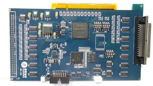
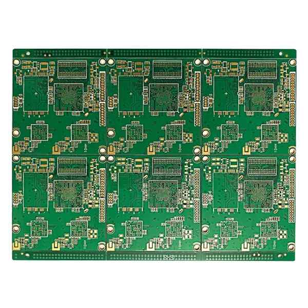
Ordinary circuit boards can be divided into single-sided wiring and double-sided wiring, commonly known as single-sided and double-sided boards. However, high-end electronic products, due to the constraints of product space design, can be stacked with multiple layers of lines inside, except for surface wiring. During the production process, after each layer of lines is made, they can be positioned and pressed by optical equipment, so that multiple layers of lines can be stacked in one circuit board. It is commonly known as multilayer PCB. Any PCB with more than or equal to 2 layers can be called a multi-layer PCB. Multilayer circuit boards can also be divided into multilayer hard circuit boards, multilayer soft and hard circuit boards, and multilayer soft and hard combination circuit boards. High precision pcb design solution for shenzhen pcb proofing manufacturer
Before designing a multilayer PCB, PCB designers need to first determine the structure of the circuit board to be used according to the size of the circuit, the size of the circuit board, and the requirements of electromagnetic compatibility (EMC), that is, decide whether to use a circuit board with 4, 6, or more layers. After determining the number of layers, determine the placement position of the inner electric layer and how to distribute different signals on these layers. This is the problem of selecting multilayer PCB stack structure. Laminated structure is an important factor affecting the EMC performance of PCB, and also an important means to suppress electromagnetic interference.


Just upload Gerber files, BOM files and design files, and the KINGFORD team will provide a complete quotation within 24h.