
Professional PCB manufacturing and assembly
Building 6, Zone 3, Yuekang Road,Bao'an District, Shenzhen, China
+86-13410863085Mon.-Sat.08:00-20:00

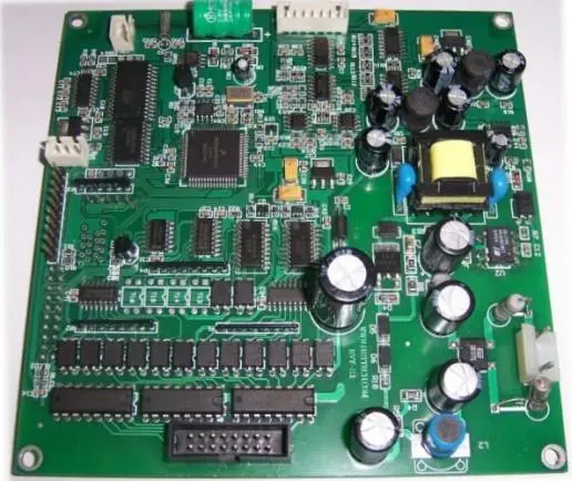
Circuit board manufacturers talk about optimizing PCB design: 1. Shorten the connection between high-frequency PCB components and reduce EMI interference. 2. Components with large weight (such as more than 20g) shall be fixed with supports and then welded. 3. Heat dissipation shall be considered for heating element to prevent element surface
Circuit board manufacturers talk about optimizing PCB design:
1. Shorten the connection between high-frequency components and reduce EMI interference.
2. Components with large weight (such as more than 20g) shall be fixed with supports and then welded.
3. Heat dissipation shall be considered for heating elements to prevent large Δ In case of defects and rework, the thermal sensor shall be far away from the heat source.
4. The arrangement of elements shall be as parallel as possible, which is not only beautiful but also easy to weld, and it is suitable for mass production. The circuit board is designed as a 4 ∶ 3 rectangle. The wire width shall not be abrupt.
Use electric soldering iron correctly
1. The electric soldering iron shall be coated with tin before use. The specific method is: heat the electric soldering iron, coat the flux when the soldering tin can be melted just now, and then evenly coat the soldering tin on the soldering iron head, so that the soldering iron head can eat a layer of tin evenly.
2. The welding time should not be too long, or the components may be damaged easily. If necessary, tweezers can be used to clamp the pins to help heat dissipation.
3. After PCB welding, clean the residual flux on the circuit board with alcohol to prevent the carbonized flux from affecting the normal operation of the circuit.
4. The electric soldering iron shall be placed on the soldering iron frame.
Summary of PCB design process defects
1、 The definition of processing level is not clear. Single sided PCB boards are designed on the TOP layer. If no instructions are given, the boards may be fabricated and installed with components without welding.
2、 The distance between the large area copper foil and the outer frame is too close. The distance between the large area copper foil and the outer frame should be at least 0.2mm. Because it is easy to cause the copper foil to rise and the solder resistance to fall off if it is milled onto the copper foil when milling the shape.
3、 Drawing a pad with a filler block Drawing a pad with a filler block can pass DRC inspection when designing a circuit, but not for processing. Therefore, such pads cannot directly generate solder resistance data. When solder resistance is applied, the filler block area will be covered by solder resistance, resulting in difficulty in device welding.
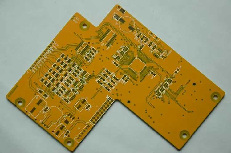
About PCB layout rules of PCB manufacturers:
1. In general, all components should be arranged on the same side of the circuit board. Only when the top layer components are too dense can some devices with limited height and low heat generation, such as chip resistance, chip capacitance, chip IC, etc., be placed on the lower layer.
2. On the premise of ensuring the electrical performance, the elements shall be placed on the grid and arranged in parallel or vertical to each other for neat and beautiful appearance. In general, the elements are not allowed to overlap; The elements shall be arranged compactly, and the elements shall be evenly distributed and uniformly spaced throughout the layout.
3. The minimum spacing between adjacent pad patterns of different components on the circuit board shall be more than 1MM.
4. The distance from the edge of the circuit board is generally not less than 2 mm. The best shape of the circuit board is rectangular, with a length to width ratio of 3:2 or 4:3. When the size of the circuit board is greater than 200 mm by 150 mm, the mechanical strength that the circuit board can withstand should be considered.


Just upload Gerber files, BOM files and design files, and the KINGFORD team will provide a complete quotation within 24h.