
Professional PCB manufacturing and assembly
Building 6, Zone 3, Yuekang Road,Bao'an District, Shenzhen, China
+86-13410863085Mon.-Sat.08:00-20:00

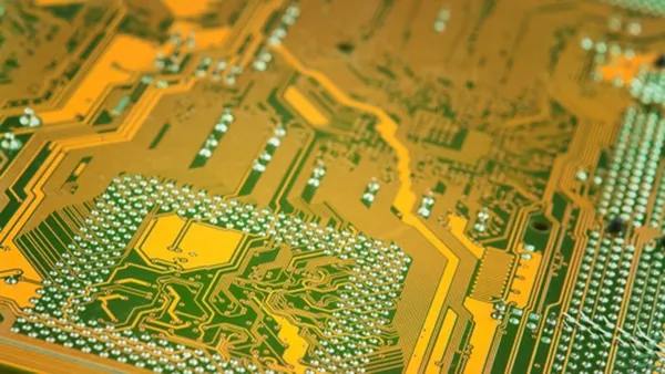
Analysis and Control of Crosstalk in High Speed PCB Design
At present, the increasingly sophisticated semiconductor technology makes the size of transistors smaller and smaller, so the signal jump edge of devices becomes faster and faster, which leads to the increasingly serious problems of signal integrity and electromagnetic compatibility in the field of high-speed digital circuit system design. Signal integrity problems mainly include transmission line effects, such as reflection, time delay, ringing, overshoot and undershoot of signals, and crosstalk between signals. Among them, signal crosstalk is the most complex, involving many factors, complex calculation, and difficult to control. Therefore, today's electronic product design urgently needs new ideas, processes, methods and technologies that are different from the traditional design environment, design processes and design methods.
EDA technology has developed a set of design and analysis tools and methodologies for high-speed PCB and circuit board level systems. These technologies cover all aspects of high-speed circuit design and analysis: static timing analysis, signal integrity analysis, EMI/EMC design, ground bounce reflection analysis, power analysis, and high-speed router. At the same time, it also includes signal integrity verification and Sig '' '' n-Off, design space detection, interconnection planning, interconnection synthesis of electrical rule constraints, as well as expert system and other technical methods, which also make it possible to solve signal integrity problems efficiently and better. Signal integrity analysis and design is the most important means of high-speed PCB board level and system level analysis and design. It plays an increasingly important role in hardware circuit design. Here, we will discuss signal crosstalk in signal integrity.
Solution of application for disturbance
The undesired noise voltage signal caused by the mutual coincidence of electromagnetic fields between signals is called signal crosstalk. If the crosstalk exceeds a certain value, it may cause circuit malfunction, which will cause the system to fail to work normally. The crosstalk problem can be solved from the following aspects:
a. Reduce the conversion rate of the signal edge when possible
Generally, when selecting devices, slow devices should be selected as far as possible while meeting the design specifications, and mixed use of different types of signals should be avoided, because fast converted signals have potential risk of crosstalk to slow converted signals.
b. Adopt shielding measures
Providing packet ground for high-speed signals is an effective way to solve the crosstalk problem. However, the package land will lead to an increase in the amount of wiring, making the originally limited wiring area more crowded. In addition, in order to achieve the expected purpose of ground wire shielding, the distance between ground points on the ground wire is critical, which is generally less than twice the length of the signal change along. At the same time, the ground wire will also increase the distributed capacitance of the signal, making the transmission line impedance increase and the signal edge slow.
c. Reasonably set up layers and wiring
Reasonably set the wiring layer and wiring spacing, reduce the length of parallel signal, shorten the spacing between signal layer and plane layer, increase the spacing between signal lines, and reduce the length of parallel signal lines (within the critical length range)
It can effectively reduce crosstalk.
d. Set up different routing layers
It is also a good way to solve crosstalk by setting different wiring layers for signals with different rates and setting plane layers reasonably.
e. Impedance matching
If the near end or far end impedance of the transmission line matches the transmission line impedance, the magnitude of crosstalk can also be greatly reduced.
The purpose of crosstalk analysis is to quickly find, locate and solve crosstalk problems in PCB implementation. General simulation tools and environment simulation analysis are independent of PCB wiring environment. After wiring, crosstalk analysis is conducted to obtain crosstalk analysis report. New wiring rules are derived and re wired, and then analysis and correction are made. This design is repeated frequently.
Through the simulation analysis, we can see that the actual crosstalk results are different, and there is a big gap. Therefore, a good tool should not only analyze crosstalk, but also apply crosstalk rules for routing. In addition, general routing tools are only driven by physical rules, and routing for crosstalk control can only be constrained by setting physical rules such as line width, line spacing, and maximum parallel routing length. The use of signal integrity analysis and design toolset ICX can support the real sense of electrical rule driven routing. Its simulation analysis and routing can be completed in one environment. During simulation, electrical rules and physical rules can be set, and signal integrity elements such as overshoot and crosstalk can be automatically calculated while routing, and routing can be automatically corrected according to the calculation results. The wiring speed is fast, and it really meets the actual electrical performance requirements.
Signal integrity design of crosstalk control
High speed PCB design rules are generally divided into two types: physical rules and electrical rules. The so-called physical rules refer to certain design rules based on physical dimensions specified by the design engineer, such as line width of 4Mi1, spacing between lines of 4Mi1, and parallel routing length of 4Mi1. The electrical rules refer to the design rules related to electrical characteristics or electrical performance, such as the wiring delay is controlled between Ins and 2ns, the total amount of crosstalk on a PCB is less than 70mV, and so on
The definition of physical rules and electrical rules can further explore high-speed router. At present, the high-speed router based on physical rules (physical rule driven) in the market includes AutoActive RE router, CCT router, B1azeRouter router and Router Editor router. In fact, these router are all physical rule driven automatic router, that is to say, they can only automatically meet the physical size requirements specified by the design engineer, It is not directly subject to the requirements of the physical dimensions of high-speed electrical, but not directly driven by high-speed electrical rules.
The high-speed router directly driven by electrical rules is very important to ensure the integrity of high-speed design signals. The design engineer always gets the electrical rules first and the design specifications are also electrical rules. In other words, our design must ultimately meet the electrical rules rather than the physical rules. The ultimate physical design implementation is the most essential to meet the electrical rule requirements of the design. Physical rules are just a conversion of electrical rules made by component manufacturers or design engineers themselves. We always expect such conversion to be equivalent and one-to-one. This is not the case.
Taking the LVDS chip as an example to complete high-speed (up to 777.76Mbps) and long-distance (up to room) data transmission, since the signal swing of LVDS technology is 3500, the general design specifications always require that the total crosstalk value on the signal line should be less than or equal to 20% of the signal swing, that is, the maximum total crosstalk is 350mV X20%=700, which is the electrical rule. The percentage of 20% depends on the noise tolerance of LVDS, It can be obtained from the reference manual.
For IS_ For Synthesizer, as long as the design engineer specifies the crosstalk value of the LVDS signal line, the wiring can be automatically adjusted and refined to ensure that the electrical performance requirements are met. During the wiring process, the design engineer will automatically consider the impact of all surrounding signal lines on the LVDS signal. For the router driven by physical rules, some hypothetical analysis and consideration are needed first. The design engineer always thinks that the crosstalk between signals only depends on the length of parallel lines between parallel signals. Therefore, some hypothetical analysis can be done in the front-end environment of high-speed circuit design, for example, it can be assumed that the length of parallel lines is 2.5 mil, and then analyze the crosstalk between them, This value may not be 70mV, but the length of parallel routing can be further adjusted according to the conclusion. If the length of parallel routing is a certain value, such as 7mi1, the crosstalk between signals is basically 70mV, Then the design engineer thinks that as long as the length of the parallel routing of the differential line pair is controlled within 7mi1, such electrical characteristic requirements can be met (the signal crosstalk value is controlled within 70mV). Therefore, the design engineer has obtained such a physical rule for high-speed PCB design during the actual physical PCB layout and routing, and the conventional high-speed router can ensure that such physical size requirements can be met.
There are two problems: first, the rule conversion is not the same. First, the crosstalk between signals is not only determined by the length of the route between parallel signals, but also depends on the flow direction of the signal, the location of the parallel line segment, whether there is a match and other factors. These factors may be difficult to predict, or even impossible to fully consider before the actual physical implementation. Therefore, after such conversion, it is not possible to ensure that the original electrical rules can be met while meeting these physical rules. This is also one of the important reasons why the PCB system still can not work normally when these high-speed wiring devices meet the rules. Secondly, it is almost impossible to consider multiple influences at the same time when these rules are converted. For example, it is difficult to consider the influence of all relevant signal lines around at the same time when considering signal crosstalk. These two aspects determine that the high-speed PCB router based on physical rules will have great problems in the design of high-speed and highly complex PCB systems, and the high-speed PCB router driven by electrical rules can better solve these problems. Summary
High speed PCB board level and system level design is a complex process. Signal integrity issues, including signal crosstalk, bring about changes in design concepts, design ideas, design processes and design means. It has become the mainstream of today's high-speed system design to ensure that problems can be found and solved quickly in the high-speed system design, and to guide the emergence of problems in the new design.


Just upload Gerber files, BOM files and design files, and the KINGFORD team will provide a complete quotation within 24h.