
Professional PCB manufacturing and assembly
Building 6, Zone 3, Yuekang Road,Bao'an District, Shenzhen, China
+86-13410863085Mon.-Sat.08:00-20:00

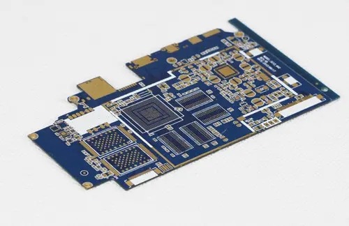
Layout of components in PCB design and key points of tablet PC PCB design
PCB assembly and PCB processing manufacturers explain the method of reasonable layout of components in PCB design and the key points of tablet PC PCB design
1.1. Aesthetic
It is not only necessary to consider the orderly placement of components, but also the graceful and smooth routing. Because ordinary laymen sometimes put more emphasis on the former in order to one-sided evaluate the advantages and disadvantages of circuit design, for the sake of product image, the former should be given priority when the performance requirements are not harsh. However, in high-performance occasions, if you have to use double-sided boards, and the circuit board is also packaged in it, you should give priority to the aesthetics of wiring.
1.2. Force
The circuit board shall be able to withstand various external forces and vibrations during installation and operation. For this reason, the circuit board should have a reasonable shape, and the positions of various holes (screw holes, special-shaped holes) on the board should be reasonably arranged. Generally, the distance between the hole and the plate edge shall be at least greater than the diameter of the hole. At the same time, it should be noted that the weakest section of the plate caused by profiled holes should also have sufficient bending strength. The connectors on the board that directly "extend" out of the equipment shell shall be reasonably fixed to ensure the reliability of long-term use.
1.3. Heating
For high-power devices with severe heat generation, in addition to ensuring heat dissipation conditions, attention should be paid to placing them in proper positions. Especially in the precise analog system, we should pay special attention to the adverse effects of the temperature field generated by these devices on the fragile preamplifier circuit. Generally, the part with very large power shall be made into a module separately, and certain thermal isolation measures shall be taken between it and the signal processing circuit.
1.4. Signal
Signal interference is the most important factor to be considered in PCB layout design. Several basic aspects are: weak signal circuit and strong signal circuit are separated or even isolated; The AC part is separated from the DC part; The high frequency part is separated from the low frequency part; Pay attention to the direction of the signal line; Layout of ground wire; Appropriate shielding, filtering and other measures. These have been repeatedly emphasized by a large number of scholars, and will not be repeated here.
1.5. Installation
It refers to a series of basic requirements put forward in specific applications to install the circuit board into the chassis, shell and slot smoothly, avoid space interference, short circuit and other accidents, and make the designated connector in the designated position on the chassis or shell. I will not repeat it here.
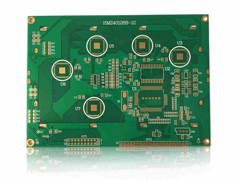
Key Points of PCB Design for Tablet PC
1. Side keys, TP, screen, headset, DC, battery, USB and other connectors should be cleared as soon as possible to prevent errors
2. All connectors such as screen, camera and touch screen are easy to reverse direction. When changing the layer of connector, it is necessary to change the position 180 degrees
3. If the parts are laid on the first layer, the second layer is the main ground, and the third layer is the copper layer for power supply. The lines shall be laid on the surface layer first, and the rest shall be laid on the third layer, and then on the second layer. The principle of the layer is to ensure the integrity of the copper layer for power supply and the layer, and the middle of the second layer shall be avoided as much as possible
4. DC-DC circuit unit, the components of each unit are placed on the same side; The input passes through the capacitor first, the output capacitor is close to the inductor, the feedback loop is far away from the inductor for interference prevention, and the input is directly connected with the output filter capacitor and the IC ground wire
5. The output line of audio power amplifier shall be isolated to prevent interference with other circuits
6. NAND FLASH has a great opportunity to use manual welding. Small parts need to be avoided, and two short circuit test points should be left on the data line
7. The audio decoding chip is difficult to be packaged and soldered as recommended, and the length of the bonding pad needs to be extended by 0.2MM
8. DC-DC circuit unit, the components of each unit are placed on the same side; The input passes through the capacitor first, the output capacitor is close to the inductor, the feedback loop is far away from the inductor for interference prevention, and the input is directly connected with the output filter capacitor and the IC ground wire
9. The HDMI signal frequency will reach more than 100M. The signal difference should be handled well. The signal processing chip and connector should be placed on the same side as far as possible
10. The side key fixed foot pad is easy to fall off and needs to be reinforced with copper
11. The device silk screen is divided into two layers, some at the top layer and some at the bottom layer. It should be unified to prevent missing silk screen PCB assembly and PCB processing manufacturers explain the key points of PCB design of tablet computer in the way of reasonable layout of components in PCB design.


Just upload Gerber files, BOM files and design files, and the KINGFORD team will provide a complete quotation within 24h.