
Professional PCB manufacturing and assembly
Building 6, Zone 3, Yuekang Road,Bao'an District, Shenzhen, China
+86-13410863085Mon.-Sat.08:00-20:00

The aesthetics should not only consider the orderly placement of PCB components, but also consider the beautiful and smooth routing of PCB. Since ordinary laymen sometimes emphasize the former to one-sided evaluate the advantages and disadvantages of circuit design, for the sake of product image, priority should be given to those with less stringent performance requirements
1、 The aesthetics should not only consider the orderly placement of components, but also consider the beautiful and smooth routing.
Because ordinary laymen sometimes emphasize the former to one-sided evaluate the advantages and disadvantages of circuit board design. For the sake of product image, the former should be given priority when the performance requirements are not harsh. However, in high-performance occasions, if you have to use a double-sided board, which is also packaged in it and cannot be seen at ordinary times, you should give priority to the aesthetics of wiring.
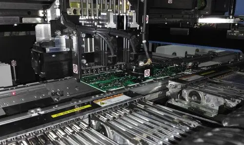
2、 The stressed circuit board shall be able to withstand various external forces and vibrations during installation and operation.
For this reason, the circuit board should have a reasonable shape, and the positions of various holes (screw holes, special-shaped holes) on the board should be reasonably arranged. Generally, the distance between the hole and the plate edge shall be at least greater than the diameter of the hole. At the same time, it should be noted that the weakest section of the plate caused by profiled holes should also have sufficient bending strength. The connectors on the board that directly "extend" out of the PCB equipment shell should be reasonably fixed to ensure the reliability of long-term use.
3、 Heating For high-power and severely heated devices, in addition to ensuring heat dissipation conditions, attention should be paid to placing them in proper positions.
Especially in the precise simulation system, we should pay special attention to the adverse effects of the temperature field generated by these PCB devices on the fragile preamplifier circuit. Generally, the part with very large power shall be made into a module separately, and certain thermal isolation measures shall be taken between it and the signal processing circuit.
4、 Signal interference is the most important factor to be considered in PCB layout design.
Several basic aspects are: weak signal circuit and strong signal circuit are separated or even isolated; The AC part is separated from the DC part; The high frequency part is separated from the low frequency part; Pay attention to the direction of the signal line; Layout of ground wire; Appropriate shielding, filtering and other measures. These have been repeatedly emphasized by a large number of scholars, and will not be repeated here.
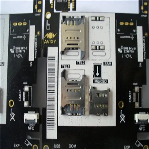
5、 Installation refers to a series of basic requirements put forward in order to install the circuit board into the chassis, shell and slot smoothly in specific applications, avoid space interference, short circuit and other accidents, and keep the designated connector in the designated position on the chassis or shell.


Just upload Gerber files, BOM files and design files, and the KINGFORD team will provide a complete quotation within 24h.