
Professional PCB manufacturing and assembly
Building 6, Zone 3, Yuekang Road,Bao'an District, Shenzhen, China
+86-13410863085Mon.-Sat.08:00-20:00

Two viewpoints on whether PCB Layout vias can be punched on pads
The circuit board manufacturer explains two views on whether vias can be punched on the pad in PCB design, and will consider punching vias on the pad of SMD components.
The design of printed circuit board is based on the circuit schematic diagram to realize the functions required by the circuit designer. The design of printed circuit board mainly refers to layout design, which needs to consider the layout of external connections. The optimal layout of internal electronic components, the optimal layout of metal wiring and through-hole, electromagnetic protection, heat dissipation and other factors. Excellent layout design can save production costs and achieve good circuit performance and heat dissipation. Simple layout design can be realized by hand, while complex layout design needs to be realized by computer aided design (CAD)
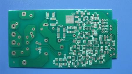
When designing PCB boards, sometimes because of the limitation of board area or the complexity of wiring, it is considered to punch vias on the pads of SMD components, which has always been divided into two opinions: support and opposition. However, in general, according to the author's years of practical experience, I feel that the way of drilling holes on the pad is easy to cause faulty soldering of SMD components, so I try to be cautious when I have to. The two views are summarized as follows.
opposition:
Generally, the SMD components can use either the reflow soldering process or the wave soldering process. The wave soldering requires that the pad density should not be too high. If the pad density is too high, it is easy to cause tin short circuit. The IC pins of the SMD are relatively dense. The reflow soldering is the preferred solution
However, the plug-in file can only use the over wave soldering method
There are many introductions about wave soldering and reflow soldering on the Internet
PCB design engineers should understand these production processes before they know how to design
There is a Fanout rule in Protel, which prohibits via from being punched on pads.
The traditional process prohibits this because the solder will flow into the vias. Now there are two processes, micro vias and plug holes, which allow vias to be placed on pads, but they are very expensive. Please consult the PCB factory.
It is better not to punch holes on PAD, which may cause false soldering. Well arrange the layout. The location of a small through-hole should still be found.
However, for SMD components, solder will flow through the via during reflow soldering. So use with caution.
support:
Generally, the purpose of making vias on the bonding pad is to enhance the over-current capability or heat dissipation. Therefore, the back is mainly paved with copper to connect the power or ground, and few patch elements are placed. In this way, to prevent tin leakage during reflow soldering, green oil can be added to the back of the vias, which solves the problem. This is how I deal with the power supply of the server motherboard. The circuit board manufacturer explains two views on whether vias can be punched on the pad in PCB design, and will consider punching vias on the pad of SMD components.


Just upload Gerber files, BOM files and design files, and the KINGFORD team will provide a complete quotation within 24h.