
Professional PCB manufacturing and assembly
Building 6, Zone 3, Yuekang Road,Bao'an District, Shenzhen, China
+86-13410863085Mon.-Sat.08:00-20:00

Function Module Segmentation in High Speed PCB Design
Most PCB boards contain some functional subsystems or areas, and each functional subsystem consists of a group of devices and their supporting circuits. For example, a typical motherboard can be divided into the following areas: processor, clock logic, memory, bus controller, bus interface, PCT bus, peripheral device interface, video/audio processing module, etc. On the one hand, all components on the PCB need to be placed closely together to shorten the routing length, reduce crosstalk, reflection, and electromagnetic radiation, and ensure signal integrity; On the other hand, the spectrum of RF energy generated by different logic devices is different. Especially in high-speed systems, the higher the signal frequency, the wider the frequency band of RF energy generated by operations related to digital signal hopping. It is necessary to prevent mutual interference between devices with different operating frequency bands, especially interference from high bandwidth devices to other devices.
The solution to the above problem is to use functional segmentation, that is, physical segmentation of subsystems with different functions on PCB. Different segmentation methods are adopted according to different products. Usually, multiple PCBs, component isolation and Layout FE isolation can be used. Proper segmentation can optimize signal quality, simplify wiring and reduce interference. The engineer must specify which functional partition a component belongs to, and this information can be obtained from the component supplier.
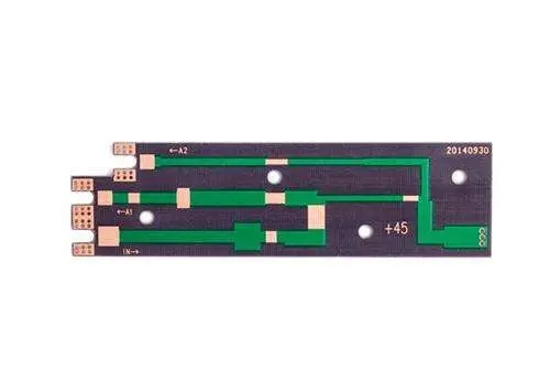
Function division can be considered as separating one functional area from another so as to isolate circuits with different functions, as shown in the example in Figure 1. In PCB design, the goal to be achieved is to limit the electromagnetic field related to the specific stator region to the region that needs this part of energy. For example, the designer hopes that the electromagnetic energy from the processor area cannot be transferred to the I/O circuit. There is a potential difference between the processor and I/O. As long as there is a potential difference, common mode energy transfer will occur between the two regions, so the division between them must be well decoupled.
The functional division needs to pay attention to two aspects: processing conducted and radiated RF energy. The conducted RF energy will be transmitted between the functional sub area and the power distribution system through the signal line, and the radiated H target will be coupled through free space. A reasonable PCB function division is to seek a reasonable scheme to transfer the useful signals to the places where they are needed and to turn away the unnecessary ones.
PCB segmentation to achieve the above functions includes two aspects: isolation and interconnection.
Isolation can be achieved by using the "trench" to form a hollow area without copper coating on all layers. The minimum width of the "trench" is 50 mils. The "trench" is like a moat, dividing the entire PCB into "islands" according to its functions. One of the functional areas (it is like an "excluded" area for those signal lines and paths on the PCB that are not connected to it). Obviously, the "trench" will divide the mirror layer to form independent power and ground for each area, which can prevent RF energy from entering from one area to another through the power distribution system.
However, segmentation is to better arrange the layout and wiring of pcbs and achieve better interconnection. It is not a complete "isolation". It must provide channels for lines that need to be connected to various sub functional areas. There are two methods: one is to use an independent transformer, optical isolator or common mode data line to cross the "trench"; the other is to build a "bridge" on the "trench". Only those signals with a "bridge pass" can enter (signal current) and exit (return current).
It is impossible to design an optimal segmentation layout. Another way is to metal shield the part that generates unexpected V energy, so as to control radiation and enhance the anti-interference ability of PCB.Circuit board assembly and circuit board processing manufacturers explain the functional module division in high-speed circuit board design


Just upload Gerber files, BOM files and design files, and the KINGFORD team will provide a complete quotation within 24h.