
Professional PCB manufacturing and assembly
Building 6, Zone 3, Yuekang Road,Bao'an District, Shenzhen, China
+86-13410863085Mon.-Sat.08:00-20:00

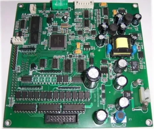
We often compare the crystal oscillator to the heart of the digital circuit. This is because all the work of the digital circuit can not be separated from the clock signal. The crystal oscillator directly controls the whole system. If the crystal oscillator does not operate, the whole system will be paralyzed. Therefore, the crystal oscillator is the prerequisite for starting the work of the digital circuit. In this paper, we will discuss with you how to do a good job of crystal oscillator layout in PCB design.
The crystal oscillator we often say is a quartz crystal oscillator and a quartz crystal resonator, both of which are made by using the piezoelectric effect of quartz crystal. Applying electric field to the two electrodes of quartz crystal will cause mechanical deformation of the crystal. On the contrary, applying mechanical pressure on both sides of the crystal will generate electric field on the crystal. Moreover, these two phenomena are reversible. Taking advantage of this feature, if alternating voltage is applied on both sides of the crystal, the chip will generate mechanical vibration and alternating electric field at the same time. This kind of vibration and electric field are generally small, but at a certain frequency, the amplitude will increase significantly, which is called piezoelectric resonance, similar to the LC circuit resonance that we often see.
How to make crystal oscillator layout in PCB design?
As the heart of digital circuits, how does crystal oscillator play a role in intelligent products? For smart home products such as air conditioners, curtains, security and monitoring, wireless transmission modules are required. They send modules from one end to the other through Bluetooth, WIFI or ZIGBEE protocols, or directly control them through mobile phones. The crystal oscillator is the core component of the wireless module, which affects the stability of the entire system. Therefore, choosing the crystal oscillator used in the system determines the success or failure of the digital circuit.
How to make crystal oscillator layout in PCB design?
Due to the importance of crystal oscillator in digital circuits, we need to be careful when using and designing:
1. There are quartz crystals inside the crystal oscillator, which are easy to be broken and damaged when impacted or dropped from the outside, thus causing the crystal oscillator to fail to vibrate. Therefore, the reliable installation of the crystal oscillator should be considered when designing the circuit, and its location should not be close to the board edge, equipment shell, etc. as far as possible.
2. During manual welding or machine welding, pay attention to the welding temperature. The crystal oscillator is sensitive to temperature. The temperature cannot be too high during PCB welding, and the heating time should be as short as possible?
The reasonable crystal oscillator layout of PCB design can suppress the system radiated interference
1、 Problem description
The product is a field camera, which is composed of five parts: core control board, sensor board, camera, SD memory card and battery. The shell is a plastic shell. The small board has only two interfaces: DC5V external power interface and USB interface for data transmission. Through the radiation test, it is found that there is a harmonic noise radiation problem of about 33MHz.
The original test data are as follows:
How to make crystal oscillator layout in PCB design?
2、 Analyze the problem
The shell structure of this product is plastic shell, which is non shielding material. Only the power line and USB line lead out of the shell during the whole machine test. Is the interference frequency radiated from the power line and USB line? Therefore, the following tests were conducted:
(1) Only the magnetic ring is added to the power line, and the test result shows that the improvement is not obvious;
(2) Only magnetic ring is added to USB cable, test result: improvement is still not obvious;
(3) Magnetic ring is added to USB cable and power cable, and the test results show that the improvement is obvious, and the interference frequency point is reduced as a whole.
It can be seen from the above that the interference frequency point is brought out from two interfaces, not the power interface or USB interface, but the internal interference frequency point is coupled to these two interfaces. Only shielding one interface can not solve the problem.
Through near-field measurement, it is found that the interference frequency point comes from a 32.768KHz crystal oscillator of the core control board, which generates strong space radiation, making the surrounding wiring and GND coupled with 32.768KHz harmonic noise, and then radiated through the interface USB cable and power cable. The problem of the crystal oscillator is caused by the following two problems:
(1) The crystal oscillator is too close to the edge of the plate, which is easy to cause radiation noise of the crystal oscillator.
(2) There are signal lines under the crystal oscillator, which may lead to harmonic noise of signal lines coupling the crystal oscillator.
(3) The filter element is placed below the crystal oscillator, and the filter capacitor and matching resistor are not arranged according to the signal flow direction, which makes the filtering effect of the filter element worse.
How to make crystal oscillator layout in PCB design?
3、 Solutions
According to the analysis, the following countermeasures are obtained:
(1) The filter capacitor and matching resistor of the crystal shall be placed close to the CPU chip and away from the board edge;
(2) Remember not to lay the floor in the crystal placement area and the projection area below;
(3) The filter capacitors and matching resistors of the crystals are arranged according to the signal flow direction, and placed neatly and compactly close to the crystals;
(4) The crystal shall be placed close to the chip, and the wiring between them shall be as short and straight as possible.
Refer to the following figure for layout:
How to make crystal oscillator layout in PCB design?
After rectification, the prototype test results are as follows:
How to make crystal oscillator layout in PCB design?
4、 Conclusion
Nowadays, many system crystal oscillators have high clock frequency and strong interference harmonic energy; In addition to conducting from its input and output lines, the interference harmonics also radiate from space. If the layout is unreasonable, it is easy to cause strong noise radiation problems, and it is difficult to solve them by other methods. Therefore, the layout of crystal oscillator and CLK signal lines is very important in PCB layout.
Considerations for PCB design of crystal oscillator
(1) The coupling capacitor shall be placed as close as possible to the power supply pin of the crystal oscillator in the following order: according to the incoming direction of the power supply, the capacitor with the smallest capacitance shall be placed as close to the power supply pin as possible.
(2) The shell of the crystal oscillator must be grounded, which can not only radiate outward, but also shield the interference of external signals on the crystal oscillator.
(3) No wiring is allowed under the crystal oscillator to ensure that the ground is completely paved. At the same time, no wiring is allowed within the 300mil range of the crystal oscillator to prevent the crystal oscillator from interfering with the performance of other wiring, devices and layers.
(4) The routing of the clock signal should be as short as possible, and the line width should be larger, so as to find a balance between the wiring length and the distance from the heat source.
(5) The crystal oscillator should not be placed on the edge of the PCB board. Pay special attention to this point during board design.


Just upload Gerber files, BOM files and design files, and the KINGFORD team will provide a complete quotation within 24h.