
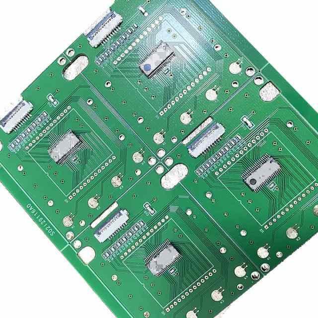
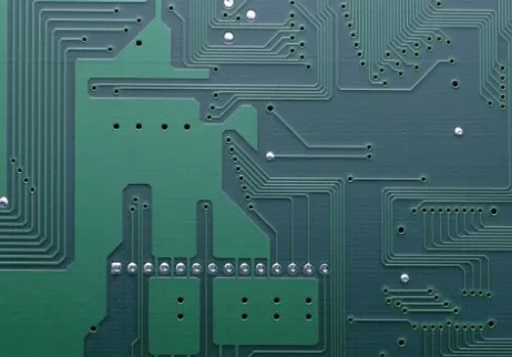
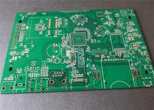
Professional PCB manufacturing and assembly
Building 6, Zone 3, Yuekang Road,Bao'an District, Shenzhen, China
+86-13410863085Mon.-Sat.08:00-20:00

Microwave Circuit PCB Design - Standing Wave and Standing Wave Coefficient
(2) Standing wave and standing wave coefficient - S parameter
1. Standing wave concept
When the load of the PCB transmission line terminal is short circuited, ZL=0, so that the amplitude of the voltage of the incident wave and the reflected wave is equal but the phase is opposite (phase difference π), so that the voltage waves of the terminal all cancel each other and become zero.
The reflection wave formed after the terminal phase shifting moves from right to left. Along the PCB transmission line, the two are added to form another wave distribution form, which is standing wave.
When a standing wave is formed on the PCB transmission line, the energy is no longer transmitted along the line, as if it is "stationed" on the PCB transmission line (corresponding to the traveling wave state). The standing wave expression of cosine voltage wave can be deduced as follows:
u=Um(t) Sin β Where Um (t)=2Um Sin ω t
It can be seen that the voltage is distributed along the PCB transmission line according to the law of simple harmonic wave, and its amplitude Um (t) changes with time, while the distribution law of nodes (points where the voltage or current is always zero) and ventral points (points with maximum values) does not change with time, thus forming periodic pulsating simple harmonic wave.
It can also be seen that the current standing wave has the same distribution rule, except that the node (or abdomen) is displaced by 1/4 wavelength, and the distance between them and the short circuit is an integral multiple of 1/4 wavelength.
2. Standing wave coefficient S (also known as voltage standing wave ratio)
In practice, the above pure standing wave does not exist. Because of the loss of PCB transmission line, the standing wave is always smaller than the traveling wave, that is, both occur at the same time. The actual asymmetry (geometric size) of PCB transmission lines also causes partial reflection of energy to generate standing waves even when the load is completely matched. That is, in practice, standing waves are non pure standing waves superimposed on traveling waves.
Pure standing wave means that the amplitude of incident wave A is equal to the amplitude of reflected wave B, that is, the reflection coefficient Г= 1 (Note: Г Complex modulus), the non pure standing wave means B<A, Г< 1。 In order to comprehensively measure various standing wave states existing on actual PCB transmission lines, the voltage standing wave coefficient - S parameter is usually used to measure.
The parameter S indicates the ratio of the ventral point voltage Umax of the standing wave of the PCB transmission line to the node voltage Umin, that is, S=Umax/Umin
It can be proved that Umax=A+B; Umin=A-B
And S=(1+ Г)/ (1- Г)
Where Г= A/B is reflection coefficient modulus, then there is Г= (S-1)/(S+1), because Г= 0~1, so the S parameter is a positive number equal to or greater than 1.
It can be seen that when the load is completely matched, Г= 0,S=1。
It can be seen from the above that the standing wave coefficient S can fully characterize the working state of high-frequency signal (especially microwave signal) transmission. In microwave circuits,
Generally, S=1.05-3.
When characterizing some components with lumped parameter characteristics, sometimes the S parameter is also called dissipation or scattering coefficient. Whether dissipative or scattering, the direct factor is standing wave. Therefore, it is most appropriate to use VSWR to characterize the S parameters of components - because VSWR can help understand the micro concepts in some circuits and measure their characteristics in combination with their incoming and outgoing PCB transmission lines.
To sum up, the microwave circuit PCB design principles are as follows:
● Standing wave is one of the root causes of instability of actual circuit or inconformity with design requirements. The design shall fully ensure that the S parameter is as close to 1 as possible, that is, the smaller the S parameter is, the better (usually S=1.05-3).
● In practice, measuring standing wave coefficient is much simpler than measuring reflection coefficient. Therefore, only standing wave coefficient is generally used in measurement technology.
● Long ground wires or overhead wires (including various forms such as tiny burrs caused by PCB design or processing) can form strong standing waves, thus forming radiated interference.
● Excessive reflected wave will interfere with signal source (including relative "source" of signal processing link).
● Standing wave interferes with normal signal transmission, reducing the signal-to-noise ratio.
● The value of S parameter depends on the reflection coefficient, that is, it depends on the transmission line characteristics of PCB and the load terminal. Therefore, in PCB design, we should not only consider the routing characteristics, but also fully consider the matching design of the transmission terminal load of each signal routing. This is the basis for ensuring circuit quality.
● Do not investigate the S parameters of components in isolation. It must be comprehensively measured in combination with their input and output signal transmission wiring, that is, it should be investigated in combination with the network of specific component combination. The circuit board assembly, circuit board design and circuit board processing manufacturers explain the microwave circuit PCB design - standing wave and standing wave coefficient.


Just upload Gerber files, BOM files and design files, and the KINGFORD team will provide a complete quotation within 24h.