
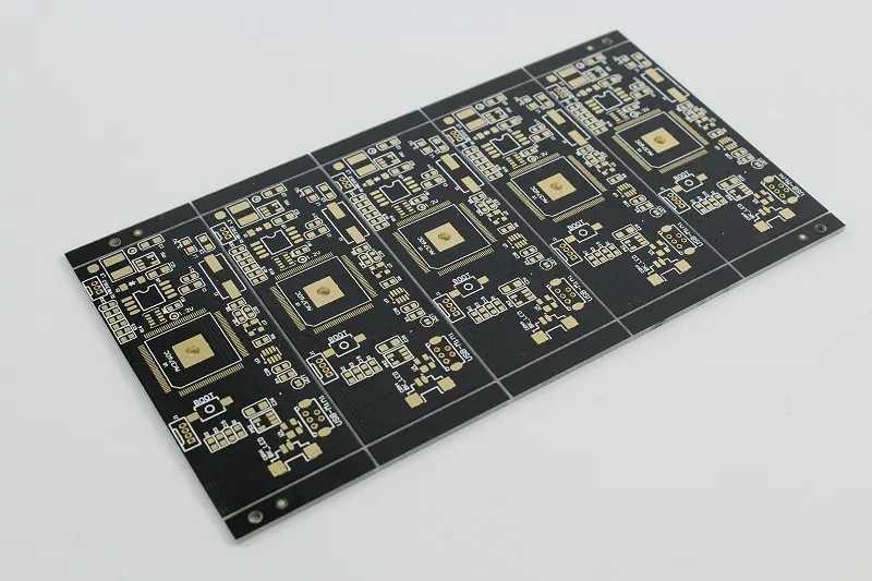
Professional PCB manufacturing and assembly
Building 6, Zone 3, Yuekang Road,Bao'an District, Shenzhen, China
+86-13410863085Mon.-Sat.08:00-20:00

Via classification, ground hole function and circuit board parallel design
The vias of pcb board can be divided into the following categories according to their functions:
1. Signal via (the via structure is required to have minimum impact on the signal);
2. Power and ground via (via structure requires the minimum distributed inductance of the via);
3. Heat dissipation via (the via structure requires the minimum thermal resistance of the via);
The functions of ground hole are as follows:
1. Heat dissipation;
2. Formation connecting multiple layers of plates;
3. Location of vias for layer change of high-speed signals;
However, the spacing of ground holes is generally only 1000 mils, and the reasons are as follows:
It is assumed that the testing range of EMI is up to 1Ghz. Then the wavelength of 1Ghz signal is 30cm, and the 1/4 wavelength of 1Ghz signal is 7.5cm=2952mil. That is, if the interval of vias can be less than 2952 mils, it can well meet the connection of the formation and play a good shielding role.
Therefore, it is generally recommended to drill through holes every 1000 mil.
Circuit Board Concurrent Design
Based on the overall process analysis of PCB design, it can be roughly divided into the following stages: netlist import, packaging and database building, master design, physical and electrical constraint design, layout, wiring, design review, and design output. For a complex design, from the perspective of the task itself, the layout and wiring are relatively heavy, especially the wiring. From the perspective of long-term practical experience, the manual wiring of important signals is still the main form of wiring.
Considering the complexity and arduousness of the layout and routing task process, the concurrent design method is considered. The parallel design methods for layout and routing are basically similar, with different objectives and priorities. The layout is taken as an example to describe the special points of parallel routing design.
Task analysis and decomposition
The starting point of layout analysis is structural design constraints and circuit topology analysis. Structural design constraints include border shape and size requirements, positioning and height limit requirements of mounting holes and special components, regional use constraints, etc.
Consider a typical design example, taking the design of mobile phone board as an example. From the view of circuit topology, the general principle block diagram is shown in Figure 1. It can be seen from Figure 1 that the signal characteristics of each part have obvious differences in the requirements for the layout. The layout of each component will be carried out according to the signal flow, while taking into account the shielding, electromagnetic compatibility (EMC) and other design requirements. For the sake of product reliability and stability, signal integrity (SI) should also be considered.
Through the analysis of the above typical design examples, we can get a method of parallel design layout: expand the circuit topology type, plan appropriate space for each component, and arrange appropriate engineers for parallel design layout.
Role arrangement
Taking Figure 1 as an example, consider the task decomposition of the following parallel design layout:
1. Communication protocol related groups, including RF components (power amplifier/transceiver/frequency converter, etc.), analog digital hybrid components, conventional analog/logic components, digital baseband processors, etc;
2. Application related group, including LCD/backlight driver, image processing engine, application processor, memory (RAM), flash memory (Flash), storage (SDCard), etc;
3. Public signal related group, including all peripheral interfaces, power supply and power management, clock components, etc.
It is assumed that each of these parallel phases is performed and completed by an engineer. The following roles are assigned: Engineer A is responsible for layout design and communication protocol group layout; Engineer B is responsible for applying relevant group layout; Engineer C is responsible for the layout of public signal related groups. The principle of role arrangement is to focus on the skills and specialties of each engineer. Circuit board design and circuit board processing manufacturer explain via hole classification and ground hole function and circuit board concurrent design.


Just upload Gerber files, BOM files and design files, and the KINGFORD team will provide a complete quotation within 24h.