
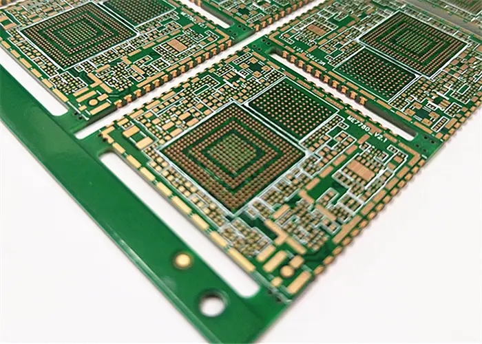
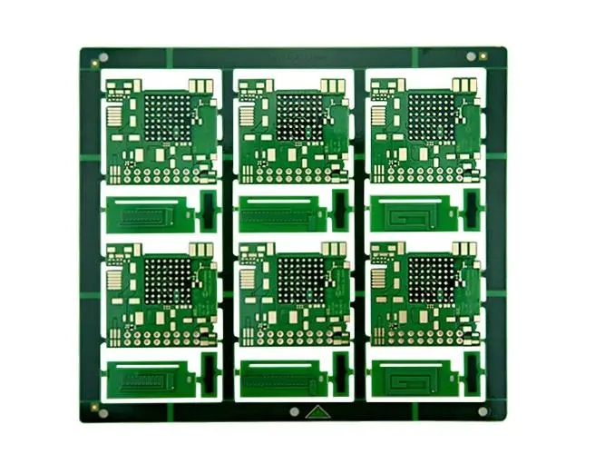
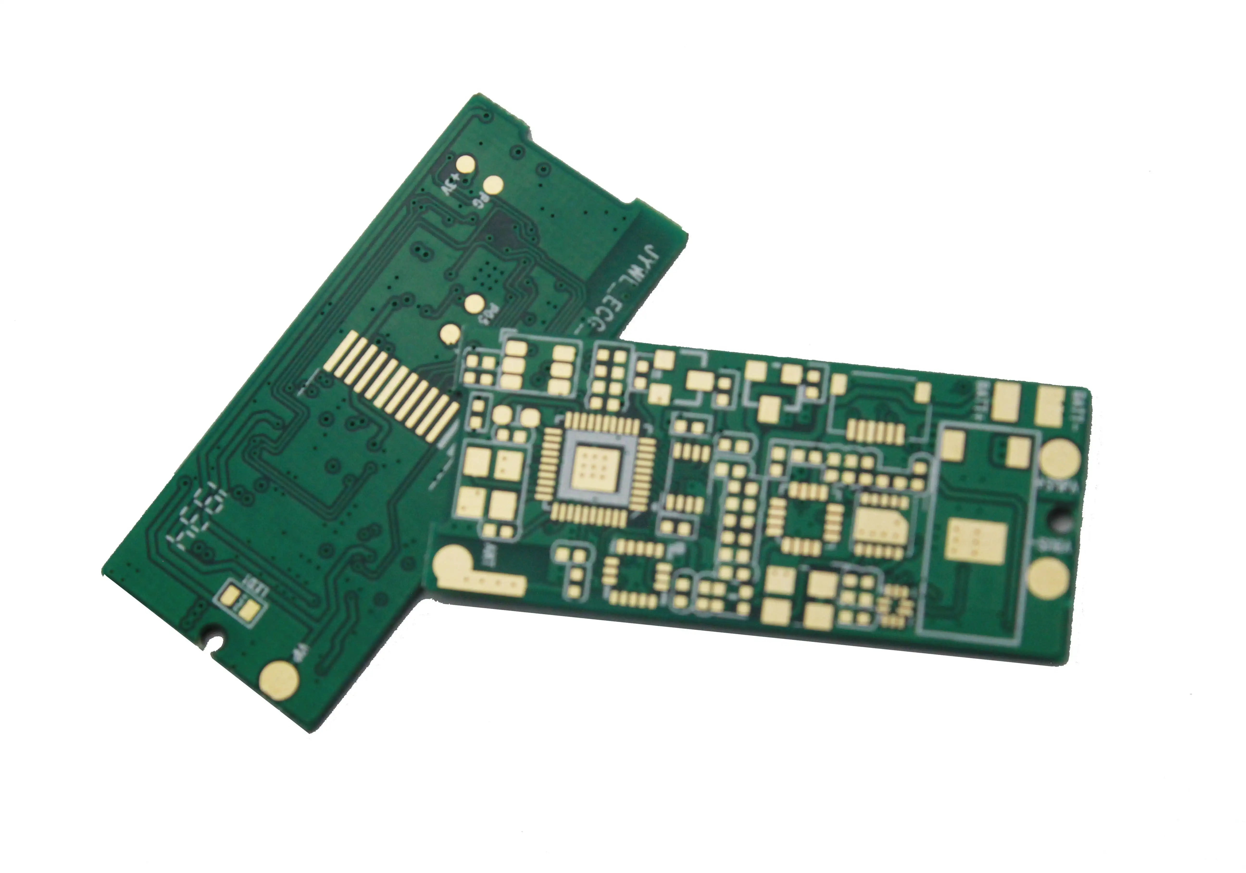
Professional PCB manufacturing and assembly
Building 6, Zone 3, Yuekang Road,Bao'an District, Shenzhen, China
+86-13410863085Mon.-Sat.08:00-20:00

PCB engineers share their experiences in PCB design
There should be a reasonable trend: such as input/output, AC/DC, strong/weak signal, high frequency/low frequency, high voltage/low voltage, etc. Their trends should be linear (or separate) and should not be mixed with each other. Its purpose is to prevent mutual interference. The best trend is straight line, but it is generally not easy to achieve. The most unfavorable trend is circular. Fortunately, isolation can be set to improve. The requirements for DC, small signal and low-voltage PCB design can be lower. So "reasonable" is relative.
2. Choose a good grounding point: the importance of a small grounding point can be seen by how many engineers and technicians have discussed it. In general, common grounding is required. For example, multiple ground wires of the forward amplifier shall be connected to the trunk ground after being converged. In reality, it is difficult to do it completely due to various restrictions, but we should try our best to follow them. This problem is quite flexible in practice. Everyone has their own set of solutions. It is easy to understand if it can be explained according to specific circuit boards.
3. Reasonably arrange power filter/decoupling capacitors: generally, only a number of power filter/decoupling capacitors are drawn in the schematic diagram, but where they should be connected is not indicated. In fact, these capacitors are set for switching devices (gate circuits) or other components requiring filtering/decoupling. These capacitors should be arranged as close to these components as possible, and will not work if they are too far away. Interestingly, when the power filter/decoupling capacitor is arranged properly, the problem of grounding point is less obvious.
4. The lines are particular: the lines that are conditionally wide should never be thin; High voltage and high frequency lines shall be round and smooth without sharp chamfers, and right angles shall not be used when turning. The ground wire should be as wide as possible, and it is better to use a large area of copper coating, which can greatly improve the docking point problem.
5. Although some problems occur in post production, they are caused by PCB design. They are: there are too many wire holes, and a little carelessness in copper sinking process will lead to hidden dangers. Therefore, wire holes shall be minimized in the design. The density of parallel lines in the same direction is too large, and it is easy to connect into one piece during welding. Therefore, the linear density shall be determined according to the level of welding process. The distance between welding points is too small, which is not conducive to manual welding. The welding quality can only be solved by reducing work efficiency. Otherwise, hidden dangers will be left. Therefore, quality and work efficiency of the welding personnel should be comprehensively considered when determining minimum distance of the welding spot.
The size of the pad or wire hole is too small, or the pad size and the drilling size are not matched properly. The former is disadvantageous to manual drilling, while the latter is disadvantageous to numerical control drilling. It is easy to drill the pad into "c" shape, or drill off the pad if it is heavy. The wire is too thin, and the large area of non wiring area is not set with copper coating, which is easy to cause uneven corrosion. That is, after the corrosion of the unrouted area, the thin wire is likely to be excessively corroded, or seemingly broken, or completely broken. Therefore, the function of copper coating is not only to increase the ground wire area and anti-interference. The above factors will greatly reduce the quality of circuit boards and the reliability of future products. Circuit board assembly, circuit board design, circuit board processing manufacturers explain the experience of circuit board engineers in PCB circuit board design.


Just upload Gerber files, BOM files and design files, and the KINGFORD team will provide a complete quotation within 24h.