
Professional PCB manufacturing and assembly
Building 6, Zone 3, Yuekang Road,Bao'an District, Shenzhen, China
+86-13410863085Mon.-Sat.08:00-20:00


How to calculate the line width and current of PCB design
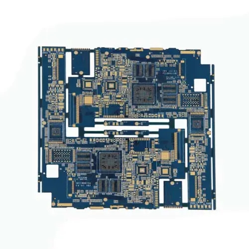
The design of printed circuit board is based on the circuit schematic diagram to realize the functions required by the circuit designer. The design of printed circuit board mainly refers to layout design, which needs to consider the layout of external connections. The optimal layout of internal electronic components, the optimal layout of metal wiring and through-hole, electromagnetic protection, heat dissipation and other factors. Excellent layout design can save production costs and achieve good circuit performance and heat dissipation. Simple layout design can be realized by hand, while complex layout design needs to be realized by computer aided design (CAD)
There are many empirical formulas about pcb line width and current, relationship tables and software networks. In the actual PCB design, it is necessary to comprehensively consider the size of the PCB, and select a suitable line width through the current.
Relationship between PCB line width and current
The calculation method is as follows:
First, calculate the sectional area of the Track. The copper foil thickness of most PCBs is 35um (if you are uncertain, you can ask the PCB manufacturer). It is the sectional area when multiplied by the line width. Note that it is converted into square millimeters.
There is an empirical value of current density, which is 15~25A/mm2. Call it the upper sectional area to get the flow capacity.
I=KT0.44A0.75
K is the correction factor. Generally, 0.024 is taken for the inner layer of copper clad wire and 0.048 is taken for the outer layer
T is the maximum temperature rise, and the unit is ℃ (the melting point of copper is 1060 ℃). A is the cross-sectional area of copper coating, and the unit is square MIL (not mm, but square mil.)
I is the maximum allowable current, in amperes (amp). Generally, 10mil=0.010inch=0.254 can be 1A, 250MIL=6.35mm, 8.3A
data
The calculation of PCB current carrying capacity has been lacking of authoritative technical methods and formulas, and experienced CAD engineers can make more accurate judgments based on their personal experience. But for CAD novices, it can be said that there is a problem.
The current carrying capacity of a PCB depends on the following factors: line width, line thickness (copper foil thickness), and allowable temperature rise. As we all know, the wider the PCB wiring, the greater the current carrying capacity.
Here, please tell me: suppose that under the same conditions, the 10 MIL cable can withstand 1A, then how much current can the 50 MIL cable withstand? Is it 5A? The answer, of course, is no. Please see the following data provided by international authorities:
The unit of line width is Inch (inch=25.4 millimeters) 1 oz. Copper=35 microns thick, 2 oz.=70 microns thick, 1 OZ=0.035 mm 1mil.=10-3 inches
Trace Carrying Capacityper mil std 275
experiment
In the experiment, the voltage drop caused by the line resistance caused by the length of the wire must also be considered. The tin on the process soldering station is only used to increase the current capacity, but it is difficult to control the volume of tin. 1 OZ copper, 1mm wide, generally used as 1 - 3A galvanometer, depending on your wire length and voltage drop requirements.
The maximum current value shall refer to the maximum allowable value under the temperature rise limit, and the fusing value is the value when the temperature rise reaches the copper melting point. Eg. The temperature rise of 50mil 1oz is 1060 ℃ (i.e. copper melting point), and the current is 22.8A. The circuit board assembly, circuit board design and circuit board processing manufacturers explain how to calculate the line width and current of PCB design.


Just upload Gerber files, BOM files and design files, and the KINGFORD team will provide a complete quotation within 24h.