
Professional PCB manufacturing and assembly
Building 6, Zone 3, Yuekang Road,Bao'an District, Shenzhen, China
+86-13410863085Mon.-Sat.08:00-20:00

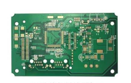
The PCB factory explains the PCB layout rules for SPS in detail
1. Drawing of circuit diagram:
a. Call out the corresponding component symbols and connect them for drawing; And assign it with the corresponding PCB Decal;
b. Check the network for errors; Whether the part number is repeated or omitted; (Filing)
c. If no error is found, turn to net list to PCB; There shall be no error report
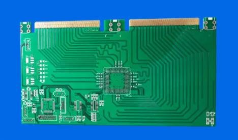
PCB processing, PCB assembly, PCB design, PCBA processing manufacturers explain PCB layout rules of PCB manufacturers for SPS
2. PCB drawing:
a. Check whether the encapsulation and the network with polar components are correct;
b. 1. Draw PCB frame with AUTO-CAD and convert it to * The dxf file is sent to the POWER PCB;
§ Note: When switching to the POWER PCB, please note that its unit should be metric system. If it is imperial system, it should be converted in AUTO-CAD in advance
2. After entering the POWER PCB, change the line width to 0.2mm, merge, and store in the library for later use;
C. Call out the PCB file first, then call out the PCB shape, set the PCB shape on the 27th layer, draw the PCB shape with the outline line, mark the size, and then start the layout
d. PCB part layout; (SPS only)
1. The layout shall be carried out according to the principle of large first, small second, vertical left to right, and four loops first;
2. First place the fixed position element, and then place the INLET, X capacitor, common mode inductor, large capacitor, MOS tube and heat sink, transformer, output rectifier and filter capacitor of the input part;
Note: The selection of heat sink and transformer will largely determine the layout of PCB, so the selection of these components should be careful
Note: For all plug-ins, horizontal components should be used as much as possible. (Because vertical components are not easy to have short circuit) The foot hole position of horizontal components should be ≥ 1mm If vertical components are not allowed to be used, deflection and short circuit shall be avoided as far as possible.
Note: For SMT components, the SMT surface should first consider the direction of the tin furnace, because this determines the direction of SMT arrangement
Note: When placing the parts on the AI surface, pay attention to whether the "FG" PIN of INLET will touch other components, such as the X capacitor. The fuse housing should be kept away from other metal housings, such as the electrolytic capacitor and high-voltage capacitor; To avoid heat transfer to the capacitor, reducing the life of the capacitor;
When placing the vertical 2W resistor, the peripheral components should be considered, and it is better to omit conduit and other things;
In terms of the bridge stack, if space is available, it is better to replace the bridge stack with four diodes;
When designing the radiator, the slightly larger radiator must be designed with more than two PIN pins; When placing MOS tube, pay attention to the shortest connection between its "D" pole and transformer; Whether it is easy to route "G" and "S";
PWM control part shall be arranged orderly, IC PWM output line shall be as short as possible, and this part shall be as far away from AC input part as possible; If there is space, the diode and voltage stabilizing tube should be plug-in as much as possible, which can be cost down
When PFC is provided, PFC IC control part shall be separated from PWM IC control part. In particular, respective GNDs shall go to the common leg of high-voltage capacitor separately. The signal line of PFC shall not be too thick
SMT capacitors, especially high-voltage SMT capacitors, should use plug-ins as far as possible, which can cost down; SMT components shall be far away from the bonding pad of AI components; In case of heavy current, necking type wiring shall be adopted;
The transformer shall be placed close to the MOT pipe and secondary components, and the distance shall be more than 3mm Special attention shall be paid to the transformer without piping. If the transformer needs to be led out with three layers of insulated wire, the wire package and iron core of the transformer are considered as primary components. Special attention shall be paid to the distance between secondary components and it shall be ensured that the distance is more than 4MM. If possible, the PIN of the transformer shall be kept as far as possible, so as to make the cumbersome transformer more solid;
The distance between TO-220 packaged rectifier tube and output filter capacitor shall be paid attention to. The output filter capacitor shall not stand against the output filter capacitor. The output capacitors shall be arranged orderly and convenient for wiring
When placing parts close to the edge, keep at least 0.5~1.0mm away from the edge, so as not to interfere with each other when connecting pieces;
The distance between the output component and the SR, understand the size of the SR and the thickness of the line; It shall be sparse but not sparse, dense but not miscellaneous, compact and neat in appearance;
At the beginning of wiring, the width of wiring is set to be 0.3 mm and the spacing is 0.3 mm. This wiring is mainly used to lay the foundation for subsequent copper laying PCB processing, PCB assembly, PCB design and PCBA processing manufacturers explain PCB layout rules of PCB manufacturers for SPS.


Just upload Gerber files, BOM files and design files, and the KINGFORD team will provide a complete quotation within 24h.