
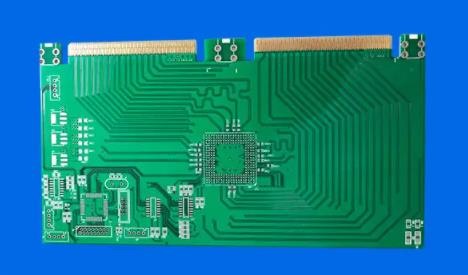
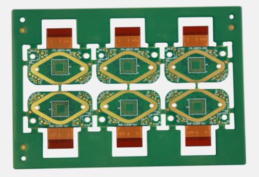
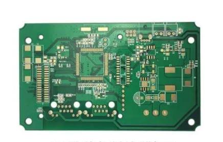
Professional PCB manufacturing and assembly
Building 6, Zone 3, Yuekang Road,Bao'an District, Shenzhen, China
+86-13410863085Mon.-Sat.08:00-20:00

Circuit board design experts talk about the shortcut of high-speed interconnection design
The research object of high-speed interconnection design is the interconnection of chips, packages, PCBs and systems. With the aid of EDA tools and advanced test and measurement equipment, it uses signal integrity, power integrity and electromagnetic field theory to provide high-speed interconnection optimization design support for engineers engaged in product system design, with the purpose of shortening the product design cycle and reducing the cost of system design, Improve the one-time pass ratio of high-speed PCB and product design.
Q: What is the biggest challenge facing engineers in the field of high-speed interconnection design?
Hu: The interconnection problems at the four levels of chip, package, board and system are closely related. In these four areas, there are still some technical details to be studied. The biggest challenge is the challenge of concept. How to think about and solve interconnection problems from the perspective of system architecture is the key to establish system design methodology. The difficulty at present is that it is difficult for an engineer to change an idea and method, which goes beyond solving technical details.
Q: What are the challenges of ideas?
Jiang: Today's products almost all include the interconnection of chips, packages, boards and systems. For example, if you only consider the interconnection problem from the board level design, but not from the whole system design, then the problem cannot be completely solved, which often leads to the prolongation of the design cycle. In the era of "fiber foam" a few years ago, optical fiber was used for everything, and some engineers used optical interfaces to realize system interconnection in wireless products. Now we have established a new scheme through simulation and test verification, combined with board level interconnection, suggesting that copper interconnection is enough for signals at 622M speed, and the cost is much saved. At present, we have sorted out the knowledge system of signal integrity to train all hardware engineers, from the concept and process to how to apply for the business of signal integrity design, and comprehensively trained engineers, and combined with the design of specific product systems to promote the upgrading of ideas.
Q: How do you integrate signal integrity design into product system design?
Liu: Before, it was very common for Huawei to invest 3-4 times on its boards. After joining the product line, the Signal Integrity Research Department mainly participated in the analysis and interconnection design of the front end, and the product engineer was responsible for the principle design. In this way, the hidden dangers of signal integrity, such as timing and crosstalk, could be found and solved in advance, thus winning time for the product to market and significantly reducing costs. Therefore, many product lines put forward the slogan of "one board success"! Now the signal integrity simulation has been embedded in each product line. At present, the signal integrity problem encountered in the product design process can be well solved by using the system design rules obtained in practice and the experience in dealing with many similar problems.
Q: How do you build your design experience?
Liu: For example, I just started working in the IBIS model testing project team. At that time, I mainly wanted to test the IBIS model used in product design, because the IBIS model is the basis of signal integrity simulation, and there are still many problems with the IBIS model provided by the industry. I wanted to establish an IBIS model library through testing to verify all models.
After testing one or two chips, it is found that this road is not feasible because each chip needs to be built with a test board, which is a very long test process. There is no way to test some high-end chips, and the project was abandoned later. However, through this project, I became an experienced IBIS model expert in a few months. The perfect signal integrity simulation tools provided by the department are very helpful for me to quickly master the system knowledge of signal integrity testing and simulation.
Q: How can an entry-level engineer be trained as an expert?
Hu: In the field of interconnection design, we have established a good resource platform, a high-speed design laboratory, and an environment for high-speed circuit simulation and testing. A novice should understand the whole field and master the basic skills in this field. Of course, it depends on whether his personal efforts can become an expert in this field?
Q: How can I work hard to become an expert engineer?
Zhang: The company has very tight requirements on the completion time of products. Every day, new problems and various application environments will emerge, forcing you to constantly study new design and simulation methods. Problems like EMI need to establish a theoretical basis for the system. I have to get up at 6:00 every morning to read classic books on electromagnetic fields and electromagnetic compatibility. Now there are many EMI problems, so I must read these books. Although the contents may not be useful, they will give you many inspirations and directions.
In addition, I often go to foreign forums. Foreign engineers have a feature. As long as you don't involve the components in specific products and only ask questions about the basic content, they will answer without reservation. This is the biggest difference between foreign engineers and domestic engineers. Foreign engineers have worked online for a long time. Although not all problems can be solved through the forum, they can give you a direction to solve problems.
When I entered the forum, I was basically in a learning state. After a period of research, I can now communicate with them.
Q: What suggestions do you have to improve the ability of engineers to design high-speed interconnection systems?
Zhang: If you want to cultivate talents, you need such an environment that engineers are happy to study technology. At the same time, you need to reach a medium level in material life. In addition, you need a good team.
From the perspective of visible standards, you should at least show up at the annual technical summit, and you must be a member of the technical summit, so that you can communicate with engineers at the international level. In terms of technical exchange, foreign engineers will tell you as long as patents and products are not involved, but domestic engineers still have the smell of blocking. I don't have much water for myself, but I can't give it to others. In fact, if the other party has no design experience, even if you tell him the whole technology, he may not be so sensitive.
Hu: To become an engineer of international level, it is not possible to close the door. We must participate in communication, which is inevitable.
Q: What is your future R&D direction?
Hu: We have done research on power integrity for 1-2 years, and the research results have been published in Designcon 2004. Now we are expanding the application of new technologies in Huawei product system design. Power integrity simulation design must be applied to low-voltage, high-speed systems. Our new situation has been opened, new tasks have come down, and new design concepts are forming. Circuit board assembly, circuit board design, and circuit board processing manufacturers explain circuit board design experts talk about high-speed interconnection design shortcuts.


Just upload Gerber files, BOM files and design files, and the KINGFORD team will provide a complete quotation within 24h.