
Professional PCB manufacturing and assembly
Building 6, Zone 3, Yuekang Road,Bao'an District, Shenzhen, China
+86-13410863085Mon.-Sat.08:00-20:00

Common Impedance and Restraint of Advanced PCB Design
PCB manufacturers, PCB designers and PCBA manufacturers explain the common impedance and suppression of advanced PCB design
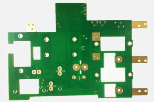
The design of printed circuit board is based on the circuit schematic diagram to realize the functions required by the circuit designer. The design of printed circuit board mainly refers to layout design, which needs to consider the layout of external connections. The optimal layout of internal electronic components, the optimal layout of metal wiring and through-hole, electromagnetic protection, heat dissipation and other factors. Excellent layout design can save production costs and achieve good circuit performance and heat dissipation.
Common resistance interference is caused by a large number of ground wires on the PCB. When two or more circuits share a section of ground wire, different circuit currents will produce a certain voltage drop on the shared ground wire, which will affect the circuit performance after being amplified; When the current frequency is very high, it will produce a lot of inductive reactance and cause the circuit to be interfered.
To suppress common impedance interference, the following measures can be taken:
(1) One point grounding
Several grounding points of unit circuits at the same level shall be concentrated as much as possible to prevent AC signals of other circuits from entering the same level, or AC signals of the same level from entering other circuits. It is applicable to low-frequency circuits with signal operating frequency less than 1MHZ. If the operating frequency is 1-1OMHz and one point grounding is adopted, the length of the ground wire shall not exceed 1/20 of the wavelength. In short, one point grounding is the basic principle to eliminate the common impedance interference of the ground wire.
(2) Nearby multipoint grounding
There are a large number of public ground wires distributed on the PCB at the edge of the board, and they present a semi closed loop (to prevent magnetic field interference). Circuits at all levels are grounded nearby to prevent the ground wire from being too long. It is applicable to high frequency circuits with signal operating frequency greater than lOMHz.
(3) Bus bar grounding
The bus bar is made of silver plated copper foil, and the ground wires of all integrated circuits on the PCB are connected to the bus bar. Busbars have the low impedance characteristics of strip symmetric transmission lines. In high-speed circuits, they can improve the signal transmission speed and reduce interference.
(4) Large area grounding
In the high-frequency circuit, all unused areas on the PCB are laid as ground wires to reduce the inductive reactance in the ground wire, thus weakening the high-frequency signal generated on the ground wire and shielding the electric field interference.
(5) Bold grounding wire
If the grounding wire is very thin, the grounding potential will change with the change of current, which will cause the timing signal level of electronic equipment to be unstable and the anti noise performance to be deteriorated, and its width shall be at least more than 3mm
(6) Ground wire separation of D/A (digital/analog) circuit
The ground wires of the two circuits are independent of each other, and then connected with the ground wire of the power supply terminal respectively to suppress their mutual interference. PCB manufacturers, PCB designers and PCBA manufacturers will explain the common impedance and suppression of advanced PCB design.


Just upload Gerber files, BOM files and design files, and the KINGFORD team will provide a complete quotation within 24h.