
Professional PCB manufacturing and assembly
Building 6, Zone 3, Yuekang Road,Bao'an District, Shenzhen, China
+86-13410863085Mon.-Sat.08:00-20:00

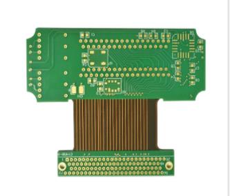
"How to place" and "how to connect" are designed for soft and hard combination boards
PCB manufacturers, PCB designers and PCBA manufacturers will explain the "how to put" and "how to connect" PCB designs in the soft and hard combination board factory
The PCB design of the soft and hard combination board factory seems complicated. It is necessary to consider the trend of various signals as well as the transmission of energy. The troubles caused by interference and heating are always with us. But in fact, the summary is very clear, which can be started from two aspects: "how to put it" and "how to connect it".
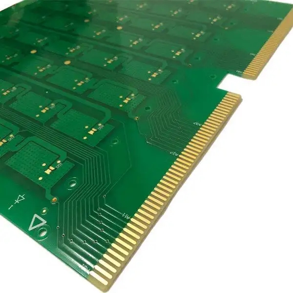
The layout principle of "large before small, difficult before easy" shall be followed, that is, the layout of important unit circuits and core components shall be given priority. This is the same as eating a buffet: the buffet has a limited appetite, and you should choose what you like first, while the PCB space is limited, and you should choose what you like first.
2. The layout shall refer to the schematic block diagram and arrange the main components according to the main signal flow direction of the board. The layout shall meet the following requirements as far as possible: the total wiring shall be as short as possible, and the key signal lines shall be as short as possible; The decoupling capacitor shall be arranged as close as possible to the power supply pin of the IC, and the loop formed between it and the power supply and ground shall be the shortest; Reduce the wrong way of signal running and prevent accidents on the road.
3. The arrangement of components should be convenient for debugging and maintenance, that is, large components should not be placed around small components, and there should be enough space around components to be debugged, which often makes it awkward to get too crowded.
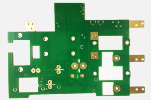
4. For circuits with the same structure, "symmetrical" standard layout shall be adopted as far as possible; The layout shall be optimized according to the standard of uniform distribution, balance of gravity and beautiful layout.
5. Plug in components of the same type shall be placed in one direction in the X or Y direction. Polarized discrete components of the same type should also strive to be consistent in the X or Y direction, so as to facilitate production and inspection.
6. The heating components shall be generally evenly distributed to facilitate the heat dissipation of the single board and the whole machine. The temperature sensitive components other than the temperature detection components shall be far away from the components with large heat.
7. High voltage, high current signal and low current, low voltage weak signal are completely separated; Separate analog signal from digital signal; High frequency signal is separated from low frequency signal; The spacing of high-frequency components shall be sufficient. In the layout of components, it shall be properly considered that components using the same power supply shall be placed together as much as possible to facilitate the separation of power supply in the future.
The above are the main considerations about "how to place", that is, layout. The "how to connect" is more complicated, which is generally:
Priority of key signal line: key signals such as small signal, high-speed signal, clock signal and synchronization signal shall be wired preferentially;
Density priority principle: start wiring from the components with the most complex connection relationship on the board. Start wiring from the area with the most dense connections on the board. PCB manufacturers, PCB designers, and PCBA manufacturers will explain the "how to put" and "how to connect" PCB designs in the soft and hard combination board factory.


Just upload Gerber files, BOM files and design files, and the KINGFORD team will provide a complete quotation within 24h.