
Professional PCB manufacturing and assembly
Building 6, Zone 3, Yuekang Road,Bao'an District, Shenzhen, China
+86-13410863085Mon.-Sat.08:00-20:00

Explanation on knowledge of designing high-speed HDI circuit board
With the increasing demand for volume of electronic products, especially the development of mobile device products in the direction of continuous miniaturization, such as the current popular Ultra Book products, and even new wearable intelligent devices, the carrier board made of HDI circuit board high-density interconnection technology must be used to further reduce the size of the terminal design.
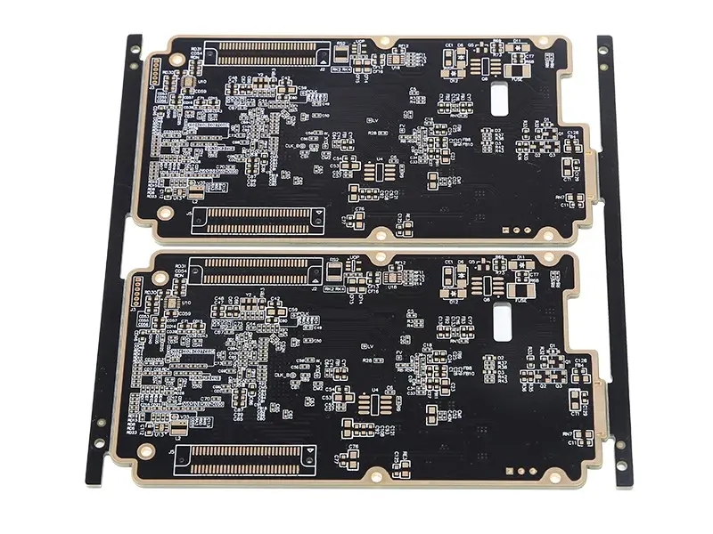
HDI circuit board is the high-density interconnection technology, which is one of the technologies used by the printed circuit board. HDI is mainly made by using the technology of micro blind hole embedding. Its feature is that it can make the distribution line density of electronic circuits in the printed circuit board higher. Due to the large increase of line density, the printed circuit board made of HDI cannot be drilled by using the general drilling method. HDI must use a non mechanical drilling process, and there are many non mechanical drilling methods. Among them, "laser hole forming" is the combination hole forming scheme of HDI high-density interconnection technology.
The application field of HDI printed circuit board is quite broad. All electronic products, such as mobile phones, ultra-thin laptops, tablets, digital cameras, automotive electronics, digital cameras, etc., have used HDI technology to reduce the motherboard design. The reduced benefits are considerable. Not only can the end product design leave more space in the organization for batteries, or more additional functional components, The cost of the product can also be relatively reduced due to the introduction of HDI.
HDI was used for middle and high price mobile phones in the early days, and now it is almost universal in all mobile devices
In the early days, the products that used the most HDI technology were mainly functional mobile phones and smart phones. These products accounted for more than half of the HDI high-density circuit boards, while the Any layer HDI (any layer high-density connector board) was a high-order HDI manufacturing process. The biggest difference between HDI circuit boards and general HDI circuit boards was that most HDI used a machine drill for PCB penetration processing for the drilling process. As for the boards between layers, Any layer HDI uses "laser" drilling to connect each layer.
For example, the Anylayer HDI production method can generally reduce the PCB volume by about 40%. At present, the Anylayer HDI has been used in Apple iPhone 4 or newer smart phones. By integrating the motherboard with higher density, the product design thickness can be reduced, so that the product design can use a lighter and thinner design style to market. However, the Anylayer HDI is manufactured by laser blind hole. It is relatively difficult to process and manufacture the circuit, and the cost is higher than that of ordinary circuit boards. At present, only high price mobile devices are used more.
HDI PCB is manufactured by Build Up method. The technical gap of HDI is the number of layers added. The more circuit layers, the higher the technical difficulty! Generally, HDI boards for general purposes can be laminated once, while HDI boards for advanced purposes can be manufactured by Build Up lamination technology in two or more times. In order to avoid damage to high-density wiring of HDI boards due to improper drilling caused by mechanical perforation, the hole forming process can simultaneously use advanced PCB manufacturing technologies such as laser perforation, electroplating hole filling, and hole stacking.
HDI shall be used for product design of key components with high number of pins
In particular, FPGA components with too many pins are a great trouble for PCB wiring. For example, the number of pins of the most common GPU components is also growing, and most of them have changed to HDI printed circuit boards for product design. HDI boards are especially suitable for design schemes that require high complex connections.
Especially for the new generation of SoC or integrated chips, its highly integrated function leads to more and more IC pins, which greatly improves the difficulty of PCB design and connection. HDI high-density circuit board design scheme can use the advantages of multi-layer interconnection and integration inside the board to connect complex chip pins one by one, while laser blind hole production can make micro blind holes in the board, which can be perforated, staggered, stacked, It can also be interconnected at any layer. The layout elasticity of the circuit is higher than that of the traditional PCB. It also provides a more easy board design scheme for integrated chip applications with a high number of pins.
The HDI circuit board design is also more complex than the previous PCB circuit board, not only the circuit has become more compact, but also the design complexity of using different layers of circuit interconnection has been greatly improved, the circuit has become thinner and more compact, which also represents that the conductor cross-sectional area of the circuit has changed less, which will lead to the transmission signal integrity problem will become more prominent, and PCB design engineers will spend more attention on board function verification and error checking.
Especially in the face of highly complex design cases, for example, the electronic circuit of the board is highly likely to encounter design changes in the development process. If the core components of the motherboard have FPGA or other components with a large number of pins, a slight design change will cause a delay in the design improvement process. How to minimize the occurrence of line deployment errors in the design process with frequent changes, Design aids that can support HDI high complexity circuit design must be matched, especially with a design architecture that can communicate FPGA logic design, hardware design, PCB logic and related design data, so that changes in design specifications of any project can immediately respond to the development system, and avoid design problems that the design board and target chip cannot match.
HDI requires high line density and needs to use laser to open holes
In fact, there is no clear definition of HDI high-density system, but generally there is a considerable difference between HDI and non HDI. First of all, the aperture used for circuit carrier boards made of HDI should be less than or equal to 6mil (1/1000 inch). As for the hole ring diameter, it should be ≤ 10mil, while the layout density of line contacts should be more than 130 points per square inch, and the line spacing of signal lines should be less than 3mil.
HDI printed circuit boards have many advantages. Because HDI circuits are highly integrated, the area of the boards used can be greatly reduced, and the higher the number of layers, the smaller the boards can be correspondingly increased. Because the size of the substrate is smaller, the area of HDI applied circuit boards can be 2 to 3 times less occupied than that of non HDI circuit boards, but can maintain the same complex circuits. The weight of natural boards can be reduced accordingly.
PCB manufacturers, PCB designers and PCBA manufacturers will explain the knowledge of designing high-speed HDI circuit boards.

Summarize the anti-static measures in PCB design
Nov 16,2022


Just upload Gerber files, BOM files and design files, and the KINGFORD team will provide a complete quotation within 24h.