
Professional PCB manufacturing and assembly
Building 6, Zone 3, Yuekang Road,Bao'an District, Shenzhen, China
+86-13410863085Mon.-Sat.08:00-20:00


PCB layer stacking technology for controlling EMI radiation
There are many ways to solve the problem of electromagnetic interference Modern EMI suppression methods include: using EMI suppression coating, selecting appropriate EMI suppression components, and electromagnetic interference simulation design Starting from the most basic<a href="/tw/" target="_blank">PCB layout, this paper discusses the role of PCB layered stacking in controlling EMI radiation and design technology
Power busbar
Proper placement of capacitors of appropriate capacity near the power supply pins of integrated circuits can make the output voltage of integrated circuits jump quickly. However, this is not the end of the problem. Due to the limited frequency response of the capacitor, the capacitor cannot generate the harmonic power required to drive the IC output cleanly in the full frequency band. In addition, the transient voltage formed on the power bus will form a voltage drop on the inductance of the decoupling path. These transient voltages are the main common mode EMI interference sources. How should we solve these problems?
As far as the integrated circuit on our circuit board is concerned, the power layer around the integrated circuit can be regarded as an excellent high-frequency capacitor, which can collect part of the energy leaked by the discrete capacitor and provide high-frequency energy for clean output. In addition, the inductance of the good power layer should be small, and the transient signal synthesized by the inductor is also small, so as to reduce common mode electromagnetic interference. Of course, the connection between the power layer and the IC power supply pin must be as short as possible, because the rising edge of the digital signal is faster and faster, it is better to directly connect to the bonding pad where the IC power supply pin is located. This needs to be discussed separately. To control common mode EMI, the power plane must be decoupled and have a sufficiently low inductance. The power plane must be a pair of well-designed power planes. Some people may ask, how good is it? The answer to this question depends on the layers of power supply, the data between layers and the operating frequency (i.e., the function of IC rise time).
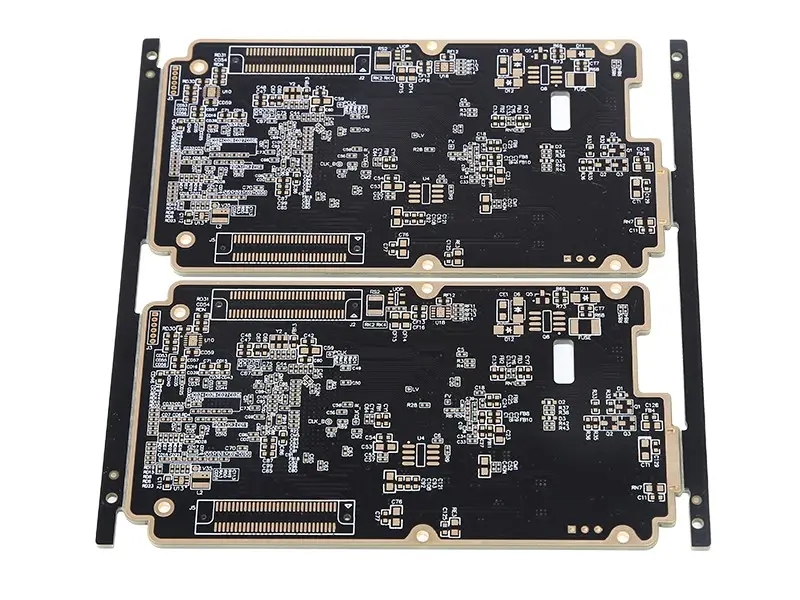
Circuit board

Generally, the power layer spacing is 6mil, the interlayer is FR4 data, and the equivalent capacitance of the power layer per square inch is about 75pF
Obviously, the smaller the layer spacing, the greater the capacitance There are not many devices with a rise time of 100 to 300 ps, but according to the current development speed of integrated circuits, devices with a rise time of 100 to 300 ps will account for a large proportion For circuits with rise times of 100 to 300 ps, 3 mil layer spacing is no longer suitable for most applications At that time, it was necessary to use layered technology with layer spacing less than 1 mil and replace FR4 dielectric material with high dielectric constant data Today, ceramics and ceramic plastics can meet the design requirements of 100 to 300 ps rise time circuits Although new materials and methods may be used in the future, for today's common 1 to 3 ns rise time circuits, 3 to 6 mil layer spacing and FR4 dielectric data, it is usually sufficient to handle high-end harmonics and make the transient signal low enough. In other words, common mode electromagnetic interference can be reduced to a very low level This PCB layered stacking design example given in this paper will assume a layer spacing of 3 to 6 mils
From the point of view of signal tracking, a good layering strategy should be to place all signal tracking on one or more layers, which are adjacent to the power layer or ground layer. For power supply, a good layering strategy should be that the power layer is adjacent to the ground layer, and the distance between the power layer and the ground layer should be as small as possible. This is what we call a "tiered" strategy.
The stacking strategy of PCB stacking helps mask and suppress EMI? The following layered superposition scheme assumes that the power supply current flows on a single layer and that a single voltage or multiple voltages are distributed in different parts of the same layer. The case of multiple power layers will be discussed later.
4-layer plate
There are several potential problems in the design of 4-ply panels. First of all, the traditional four layer plate with a thickness of 62 mils, even if the signal layer is in the outer layer and the power layer and the grounding layer are in the inner layer, the distance between the power layer and the grounding layer is still too large.
If the cost requirement is the first, you can consider the following two traditional 4-layer board alternatives. These two solutions can improve EMI suppression efficiency, but they are only applicable to applications where the density of components on board is low enough and there is enough area around the components (to place the required power copper layer). The first is the preferred solution. The outer layer of PCB is the ground plane, and the middle two layers are the signal/power layer. The power supply on the signal layer adopts wide wire wiring, which can make the path impedance of the power supply current low, and the impedance of the signal microstrip path low. From the perspective of EMI control, this is the best 4-layer PCB structure available. In the second scheme, the outer layer uses power and ground, and the middle two layers use signals. Compared with the traditional 4-layer plate, the improvement is small, and the interlayer impedance is as poor as the traditional 4-layer plate. If the trace impedance is to be controlled, the above superposition scheme must be very careful to arrange the trace under the power supply and grounding copper island. In addition, the copper islands on the power supply or ground plane should be interconnected as much as possible to ensure DC and low-frequency connections.
6-layer plate
If the component density on the 4-ply board is relatively high, it is better to use the 6-ply board. However, some stacking schemes in the 6-layer board design are not enough to mask the electromagnetic field, and have little effect on reducing the transient signal of the power bus.
10 ply board
Due to the very thin insulation layer between multiple layers of boards, the impedance between layers 10 or 12 of this circuit board is very low. As long as there is no problem with layering and stacking, good signal integrity can be achieved. It is more difficult to manufacture 12 ply plates with a thickness of 62mil, and there are few manufacturers that can process 12 ply plates.
If such tight through-hole is not available, the inductance will increase, the capacitance will decrease, and the electromagnetic interference will certainly increase When the signal wire must leave the PCB wiring layer and be connected to other wiring layers through vias, the grounding vias should be placed near the vias so that the loop signal can be returned to the appropriate ground plane smoothly The signal loop will return from the power layer or the ground layer (that is, the 5th or 6th layer), because the capacitive coupling between the power layer and the ground layer is good, the signal is easy to transmit


Just upload Gerber files, BOM files and design files, and the KINGFORD team will provide a complete quotation within 24h.