
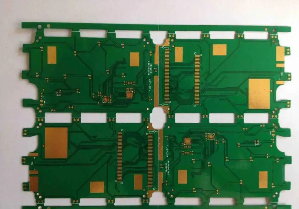
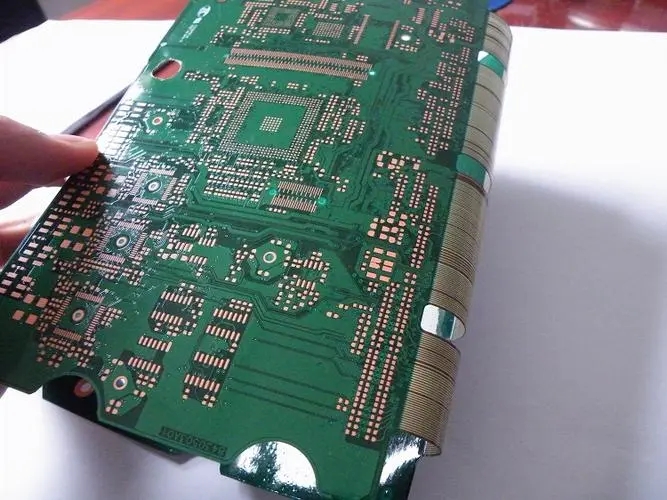
Professional PCB manufacturing and assembly
Building 6, Zone 3, Yuekang Road,Bao'an District, Shenzhen, China
+86-13410863085Mon.-Sat.08:00-20:00

The essence of PCB design is all here. Collect and use it quickly
1、 Data to be provided by hardware
1. The accurate schematic diagram includes written documents, electronic files and correct network table;
2. Formal BOM with component code. For components not in the package library, the hardware engineer shall provide DATASHEET or real objects, and specify the definition order of pins;
3. Provide the general layout of PCB or the placement of important units and core circuits. Provide PCB structure diagram, which shall indicate PCB shape, mounting hole, positioning element, prohibited layout area and other relevant information;
2、 Basic design requirements
1. High current components and networks above 1A;
2. Important clock signals, differential signals and high-speed digital signals;
3. Analog small signal and other easily interfered signals;
4. Other signals with special requirements;
3、 Description of special requirements
1. Differential distribution line, shielding network, characteristic impedance network, equal delay network, etc;
2. Prohibited wiring area of special components, solder paste offset, solder mask windowing and other special requirements for structures;
3. Read the schematic diagram carefully, understand the circuit architecture, and understand the working conditions of the circuit;
4. On the basis of full communication with the hardware engineer, confirm the key network in PCB and understand the design requirements of high-speed components;
4、 Packaging of fixed components
1. Open the network table and browse all the packages to ensure that the packages of all components are correct and the component library contains the packages of all components. All information in the network table is capitalized, and problems are found when loading, or PCB BOMs are discontinuous. The specific names of components are uniformly named according to the company's specifications;
2. All standard components are packaged in the company's unified component library;
3. For packages that do not exist in the component library, the hardware engineer shall provide the component DATASHEET or the physical object shall be built by a specially assigned person for confirmation;
5、 Create PCB frame
1. Create PCB file according to PCB structure diagram or corresponding template, including relevant information such as mounting hole and forbidden layout area;
2. Dimensions. The precise structure of PCB shall be indicated in the drilling layer, and no closed dimension can be formed;
6、 Import Network Table
1. Import the netlist and eliminate all loading problems. Each EDA software has its own differences. You can query the relevant tutorials for specific solutions;
2. If EDA software is used, the netlist must be imported more than twice (without any prompt message) to confirm that the import is correct;
7、 PCB layout
1. First, determine the reference point. Generally, the reference point is set at the intersection of the left and bottom border lines (or the intersection of extension lines) or the first pad of the PCB plug-in;
2. Once the reference point is determined, the component layout and routing shall be based on this reference point. 10-25 MIL grid is recommended for layout;
3. Fix and lock all components with positioning requirements as required;
4. Basic principles of layout:
① Follow the principle of "hard before easy, big before small";
② The layout can refer to the schematic diagram and general layout provided by the hardware engineer, and the main original devices can be placed according to the signal flow direction;
③ The overall connecting line shall be as short as possible, and the key signal line shall be the shortest;
④ Strong signal, weak signal, high voltage signal and weak voltage signal shall be completely separated;
⑤ High frequency element spacing shall be sufficient;
⑥ Separate analog signal and digital signal;
5. Symmetrical layout shall be adopted for circuits with the same structure as far as possible;
6. Optimize the layout according to the standard of uniform distribution, balance of gravity and beautiful layout;
7. Components of the same type should be consistent in the X or Y direction. The same type of polar discrete components should also strive to be consistent in the X or Y direction, so as to facilitate production and commissioning;
8. The placement of components shall be convenient for debugging and maintenance. Small components shall not be placed beside large components. There shall be enough space around the components to be debugged. The heating element shall have enough space for heat dissipation. The thermal element shall be far away from the heating element;
9. The distance between dual in-line elements shall be greater than 2mm. The distance between BGA and adjacent elements is greater than 5mm. The mutual distance between small elements such as resistor and capacitor is greater than 0.7mm. The outer side of the patch element pad and the outer side of the adjacent plug-in element pad shall be more than 2mm. The original components cannot be inserted 5 mm around the crimping components. No mounting components can be placed within 5 mm around the welding surface;
10. The decoupling capacitor of the integrated circuit shall be as close to the power supply pin of the chip as possible, and the high-frequency shall be as close as possible. Make it form the shortest loop with the power supply and ground;
11. The bypass capacitor shall be evenly distributed around the integrated circuit;
12. During component layout, components using the same type of power supply shall be put together as much as possible to facilitate future power distribution;.
13. The placement of resistance capacitance devices for impedance matching purposes shall be reasonably arranged according to their attributes;
① The layout of matching capacitance and resistance shall be clearly distinguished. For multi load terminal matching, it must be placed at the farthest end of the signal for matching;
② The matching resistor shall be arranged close to the driving end of the signal, and the distance shall not exceed 500 MIL generally;
14. Adjust characters. All characters shall not be put on the wall, and the character information shall be clearly visible after assembly. All characters shall be consistent in X or Y direction. The size of characters and silk screen shall be uniform;
15. Place the MARK point of PCB;
8、 PCB wiring
1. Routing Priorities
① Density loose principle: start wiring from the devices with simple connection relationship on the PCB, and start wiring from the area with the most loose connection to adjust personal status;
② Core priority principle: For example, core parts such as DDR RAM shall be wired preferentially, and similar signal transmission lines shall be provided with special layer, power supply and ground loop; Other secondary signals shall take the whole into consideration and shall not conflict with the key signals;
③ Priority of key signal lines: power supply, analog small signal, high-speed signal, clock signal, synchronization signal and other key signals shall be laid in priority;
2. Ground wire loop rules:
The minimum rule of the loop is that the loop area formed by the signal line and its loop should be as small as possible. The smaller the loop area, the less external radiation and the less external interference it receives. In view of this rule, when dividing the ground plane, we should consider the distribution of ground plane and important signal routing to prevent problems caused by slotting in the ground plane: in the design of double-layer board, when leaving enough space for power supply, we should fill the remaining part with reference ground, add some necessary vias, effectively connect the double-sided signals, and try to use ground wire to isolate some key signals, For some designs with high frequency, the ground plane signal loop should be specially considered, and it is recommended to use multilayer boards;
3. Tamper control:
The mutual interference between different networks on PCB caused by long parallel wiring is mainly due to the distributed capacitance and inductance between parallel lines. The main measures to overcome the interference are to increase the spacing of parallel wiring and follow the 3W rule;
4. Shielding protection:
The corresponding ground wire circuit rules are actually designed to minimize the circuit area of signals, and are mostly used for some important signals, such as clock signals and synchronous signals. For signals that are particularly important and have a high frequency, the copper shaft cable shielding structure design should be considered, that is, the lines laid are separated by ground wires, and how to effectively combine the shielding ground with the actual ground plane should also be considered;
5. Routing direction control rules:
The routing direction of adjacent layers is orthogonal, so as to avoid different signal lines running in the same direction in adjacent layers, so as to reduce unnecessary inter layer interference; When it is difficult to avoid this situation due to the restriction of plate structure, especially when the signal speed is high, it is necessary to consider to use the ground plane to isolate each wiring layer and the ground signal line to isolate each signal line;
6. Impedance matching rules:
The wiring width of the same network shall be consistent. The change of the line width will cause the nonuniform characteristic impedance of the line. When the transmission speed is high, reflection will occur. This situation should be avoided as far as possible in the design. Under some conditions, such as connector lead out and BGA packaged lead out with similar structure, it may be impossible to avoid the change of line width, and the effective length of the inconsistent part in the middle should be reduced as much as possible;
7. Routing length control rules:
The routing length control rule is the short line rule. The routing length should be kept as short as possible during the design to reduce the interference caused by the routing length. In particular, some important signal lines, such as clock lines, must be placed close to the device. For driving multiple devices, the network topology structure shall be determined according to the specific situation;
8. Chamfer rules:
In PCB design, sharp corners and right angles should be avoided to generate unnecessary radiation and poor process performance. The included angle between all lines shall be ≥ 135 °;
9. Integrity rules of power and ground layers:
For the area with dense through holes, pay attention to avoid the interconnection between the holes in the hollowed out area of the power supply and the stratum, forming the division of the plane layer, thus damaging the integrity of the plane layer, and thus causing the increase of the loop area of the signal line in the stratum;
10. 3W rule:
In order to reduce the interference between lines, it is necessary to ensure that the line spacing is large enough. When the line center distance is not less than 3 times the line width, 70% of the electric fields can be kept from interfering with each other, which is called the 3W rule. If 98% electric fields do not interfere with each other, the 10W rule can be used;
11. Rule 20H:
Because the electric field between the power layer and the stratum is variable, electromagnetic interference will be radiated at the edge of the board. It is called edge effect. The power layer can be shrunk in such a way that the electric field is only conducted within the range of the ground plane. In the unit of one H (the thickness of the medium between the power supply and the ground), 70% of the electric field can be limited to the grounding edge if it is reduced by 20H; Shrinking 100H can limit 98% of the electric field;
9、 Arrange stacking order
1. In the high-speed digital circuit, the power supply and the stratum should be close together as far as possible, and no wiring should be arranged in the middle. All wiring layers shall be close to one plane as far as possible, and the ground plane shall be preferred as the isolation layer;
2. In order to reduce the interference between signals, the signal direction of adjacent wiring layers shall be perpendicular to each other. If the same direction cannot be avoided, the overlapping of signals in the same direction of adjacent signal layers shall be avoided;
3. Several impedance layers can be set as required. The impedance layer should be clearly marked as required. Pay attention to the selection of reference layers. Arrange all signals with impedance requirements on the impedance layer;
The circuit board manufacturing, circuit board design and PCBA processing manufacturers will explain the essence of PCB design to you here. Collect and use it quickly.


Just upload Gerber files, BOM files and design files, and the KINGFORD team will provide a complete quotation within 24h.