
Professional PCB manufacturing and assembly
Building 6, Zone 3, Yuekang Road,Bao'an District, Shenzhen, China
+86-13410863085Mon.-Sat.08:00-20:00

Using New Thinking and New Understanding to Strengthen PCB Design of High Speed Circuit
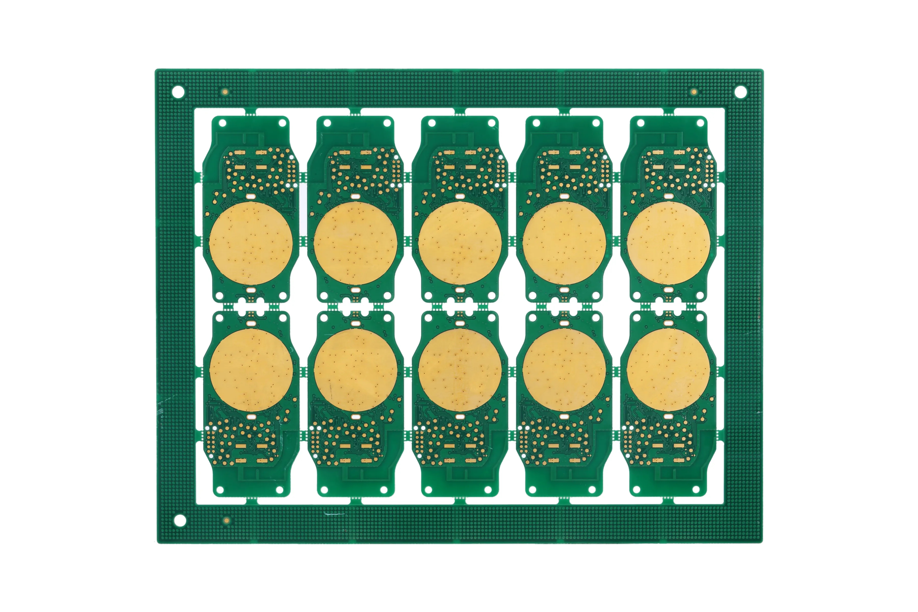
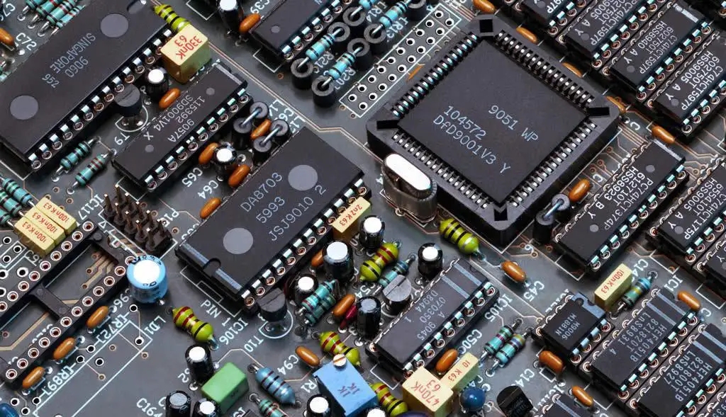
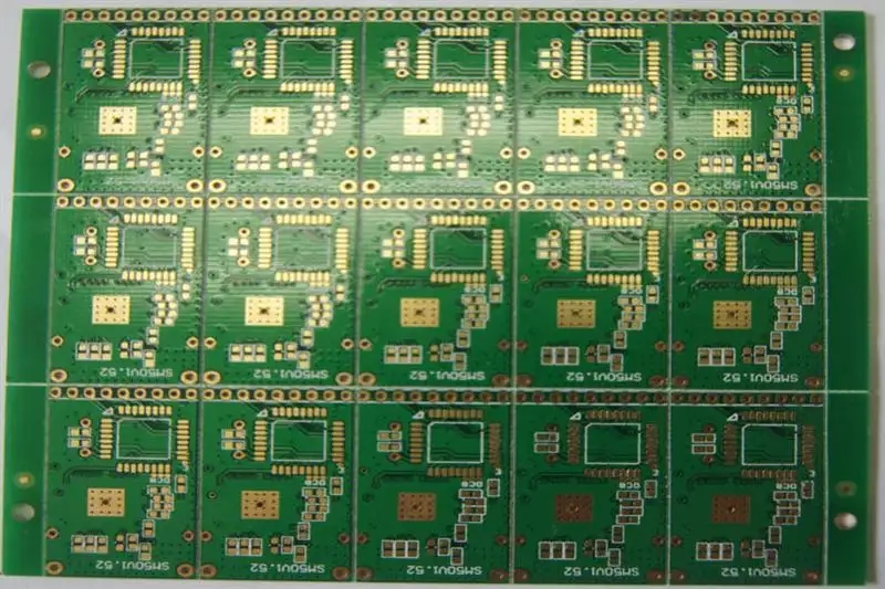
The PCB circuit board is mainly made of insulating board as the base material, cut into a certain size according to the requirements, attached with a conductive pattern and arranged with holes, to replace the chassis of the electronic components of the previous device, and realize the interconnection between the electronic components. The digital signal in PCB design circuit jumps quickly. It is generally agreed that when the rise or fall time of the digital signal is less than 5% of the signal cycle, it is called a high-speed circuit. It is generally believed that if the frequency of digital logic circuit reaches or exceeds 50MHz and the circuit working at this frequency accounts for more than 1/3 of the whole system, it is called high-speed circuit. PCB circuit board design of high-speed circuit can not be as simple as PCB design of low-speed circuit. It is necessary to add some new knowledge and new thinking to avoid and reduce the above situations. There are the following considerations for high-speed circuit PCB design.
First, signal integrity. Before any circuit PCB design, the integrity of all signals in the system after the completion of circuit PCB design should be considered. This is more important in high-speed circuit PCB design. If not fully considered in advance, it is very easy to cause serious damage to the quality of all signals in the system, or the integrity of signals will be easily damaged.
Secondly, timing coordination. The timing coordination is mainly reflected in the violation of the standard of the signal establishment time and holding time, the failure of the minimum pulse width to meet the requirements, and the phase overlap caused by multi-phase clocks in the system. In the design of high-speed circuit PCB, the cycle of the signal is generally only ns wide. At this time, it is not easy to ensure the accurate coordination between the clock signal and the data signal. In addition, the device itself has more or less drift and dispersion of various parameters, which makes it more difficult to achieve mutual coordination between different timing signals. In view of the above, the PCB design of high-speed circuit should first consider the functional simulation verification before PCB design, and carefully analyze theoretically whether each signal can meet the expected indicators. The second is to check whether each component in the sequential circuit meets its own timing requirements. For all involved components, high-frequency testing instruments should be used to carefully check and verify each parameter of the component itself.
Finally, electromagnetic interference. Electromagnetic interference of electrical equipment is another important aspect in PCB design of high-speed circuit. The outstanding performance of EMI in high-speed circuits is that when the digital system is powered on, it radiates certain electromagnetic waves to the surrounding environment, thus interfering with the normal work of other electronic equipment in the surrounding environment. The main reasons for EMI are that the working frequency of the circuit is too high, the signal changes too quickly, and the layout and wiring are unreasonable.
The consideration of signal integrity and EMI is different from that of conventional low-speed circuit PCB design. The inherent PCB design idea tends to pursue the optimization of a single signal, while today's high-speed circuit PCB design field emphasizes the optimization of overall performance. In low speed circuit PCB design, we often pursue some key signals, such as the waveform optimization of clock signal, so many PCB designers will add Schmidt trigger or some BUF to shape the required signal when encountering such signals. In today's high-speed circuit PCB design field, the more standard digital signal, the shorter its rise time and fall time, the faster the signal jumps, and contains more high-order harmonic components. All these high-frequency components are more likely to generate external radiation, and ultimately cause the deterioration of the surrounding signal quality, making the overall signal difficult to achieve optimal. Therefore, in the high-speed circuit PCB design, if the level of a signal jumps too fast, the solution is often to add a corresponding filter circuit or RTC (rise time controller) circuit to slow down the change of the signal, so as to ensure the optimization of the overall signal.
PCB manufacturers, PCB designers and PCBA manufacturers explain how to use new thinking and new understanding to strengthen high-speed PCB design.


Just upload Gerber files, BOM files and design files, and the KINGFORD team will provide a complete quotation within 24h.