
Professional PCB manufacturing and assembly
Building 6, Zone 3, Yuekang Road,Bao'an District, Shenzhen, China
+86-13410863085Mon.-Sat.08:00-20:00

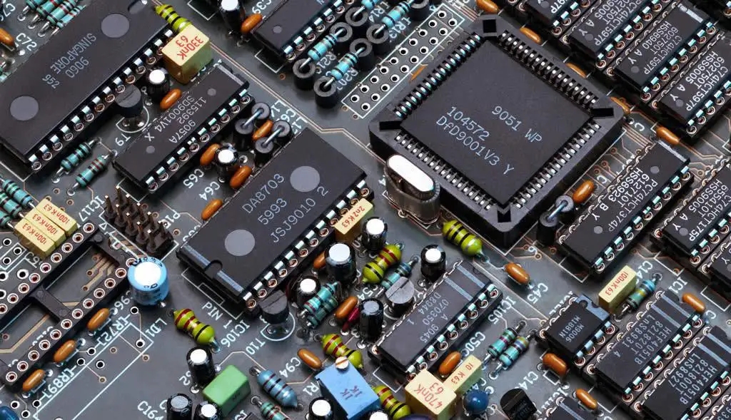
Pcb circuit board component wiring and anti-interference capability and electromagnetic compatibility?
1. No wiring is allowed in the area ≤ 1mm from the drawn wiring area to the PCB edge and 1mm around the mounting hole;
2. The power cord shall be as wide as possible and shall not be less than 18mil; The signal line width shall not be less than 12 mil; CPU incoming and outgoing lines shall not be less than 10mil (or 8mil); Line spacing shall not be less than 10mil;
3. Normal through-hole shall not be less than 30mil;
4. Double in-line insertion: pad 60ml, aperture 40ml;
1/4W resistance: 51 * 55mil (0805 meter sticker); When inserting in line, the pad is 62mil, and the hole diameter is 42mil;
Stepless capacitance: 51 * 55mil (0805 meter sticker); When directly inserting, the pad is 50mil, and the hole diameter is 28mil;
5. Note that the power line and ground wire should be radial as far as possible, and the signal line should not be looped.
How to improve anti-interference ability and electromagnetic compatibility?
How to improve anti-interference ability and electromagnetic compatibility when developing electronic products with processors?
1. The following systems shall pay special attention to anti electromagnetic interference:
(1) The microcontroller has a very high clock frequency and a very fast bus cycle.
(2) The system contains high-power, high current drive circuits, such as spark generating relays, high current switches, etc.
(3) The system includes weak analog signal circuit and high-precision A/D conversion circuit.
2. The following measures shall be taken to increase the anti electromagnetic interference capability of the system:
(1) Microcontroller with low frequency shall be selected:
Microcontroller with low external clock frequency can effectively reduce noise and improve the anti-interference ability of the system. For square wave and sine wave with the same frequency, the high-frequency component in square wave is much more than that in sine wave. Although the amplitude of the high-frequency component of the square wave is smaller than that of the fundamental wave, the higher the frequency, the easier it is to emit as a noise source. The most influential high-frequency noise generated by the microcontroller is about three times the clock frequency.
(2) Reduce distortion in signal transmission
Microcontrollers are mainly manufactured with high-speed CMOS technology. The static input current of the signal input terminal is about 1mA, the input capacitance is about 10PF, and the input impedance is quite high. The output terminal of the high-speed CMOS circuit has a considerable load capacity, that is, a considerable output value. If the output terminal of a gate is led to the input terminal with a relatively high input impedance through a long line, the reflection problem is very serious, which will cause signal distortion and increase system noise. When Tpd>Tr, it becomes a transmission line problem, and signal reflection, impedance matching and other problems must be considered.
The delay time of the signal on the PCB is related to the characteristic impedance of the lead, that is, the dielectric constant of the PCB material. It can be roughly considered that the transmission speed of the signal in the PCB lead is about 1/3 to 1/2 of the speed of light. Tr (standard delay time) of common logic telephone elements in the system composed of microcontroller is between 3 and 18 ns.
On the printed circuit board, the signal passes through a 7W resistor and a 25cm long lead, and the line delay time is about 4~20ns. That is to say, the shorter the lead of the signal on the printed line, the better, and the maximum length should not exceed 25cm. And the number of vias should be as small as possible, preferably no more than 2.
When the rise time of the signal is faster than the signal delay time, it should be processed according to fast electronics. At this time, the impedance matching of the transmission line should be considered. For the signal transmission between the integrated blocks on a printed circuit board, the Td>Trd should be avoided. The larger the printed circuit board, the faster the system cannot be.
Summarize a rule of PCB design with the following conclusions:
When the signal is transmitted on the printed board, its delay time shall not be greater than the nominal delay time of the device used.
(3) Reduce cross interference between signal lines:
A step signal with rise time of Tr at point A is transmitted to end B through lead AB. The delay time of signal on AB line is Td. At point D, due to the forward transmission of point A signal, the signal reflection after arriving at point B and the delay of line AB, a page pulse signal with a width of Tr will be induced after Td time. At point C, due to the transmission and reflection of the signal on AB, a positive pulse signal with a width twice the delay time of the signal on AB line will be induced, that is, 2Td. This is cross interference between signals. The strength of the interference signal is related to the di/at of the C point signal and the distance between lines. When the two signal lines are not very long, what you see on AB is actually the superposition of two pulses.
The micro control made by CMOS process has high input impedance, high noise and high noise tolerance. The digital circuit does not affect its operation if it is superposed with 100-200mv noise. If line AB in the figure is an analog signal, such interference will become intolerable. If the printed circuit board is a four layer board, one of which is a large area of ground, or a double-sided board, and the reverse side of the signal line is a large area of ground, the cross interference between signals will be reduced. The reason is that the characteristic impedance of the signal line is reduced in a large area, and the reflection of the signal at the D terminal is greatly reduced. The characteristic impedance is inversely proportional to the square of the dielectric constant of the medium between the signal line and the ground, and is proportional to the natural logarithm of the thickness of the medium. If the AB line is an analog signal, the interference of the digital circuit signal line CD to AB should be avoided. There should be a large area of ground below the AB line, and the distance between the AB line and the CD line should be 2-3 times greater than the distance between the AB line and the ground. The local shielding ground can be used, and the ground wire can be laid on the left and right sides of the lead wire with the bonding.
(4) Reduce noise from power supply
The power supply not only provides energy for the system, but also adds its noise to the power supply. The reset line, interrupt line and other control lines of the microcontroller in the circuit are most vulnerable to the interference of external noise. The strong interference on the power grid enters the circuit through the power supply. Even in the battery powered system, the battery itself also has high-frequency noise. The analog signal in the analog circuit can not withstand the interference from the power supply.
extension
(5) Pay attention to the high-frequency characteristics of printed wire boards and components
In the case of high frequency, the lead, via, resistance, capacitance, distributed inductance and capacitance of connectors on the printed circuit board cannot be ignored. The distributed inductance of capacitance and the distributed capacitance of inductance cannot be ignored. The resistance will reflect the high-frequency signal, and the distributed capacitance of the lead will play a role. When the length is greater than 1/20 of the corresponding wavelength of the noise frequency, the antenna effect will be generated, and the noise will be transmitted outward through the lead.
The via of the printed circuit board causes a capacitance of about 0.6 pf.
A 2-6pf capacitor is introduced into the packaging material of an integrated circuit itself.
A connector on a circuit board has 520nH distributed inductance. A 24 pin integrated circuit block with double row straight cut is introduced with 4~18nH distributed inductor.
These small distributed parameters can be ignored in this low frequency microcontroller system; Special attention must be paid to high-speed systems.
(6) Element layout shall be reasonably divided
Anti electromagnetic interference shall be fully considered for the position of components arranged on the printed circuit board. One of the principles is that the lead wires between components shall be as short as possible. In terms of layout, the analog signal part, high-speed digital circuit part and noise source part (such as relay, large current switch, etc.) shall be reasonably separated to minimize the signal coupling between them.
(7) Handle the grounding wire
On the printed circuit board, the power cord and ground wire are the most important. The most important way to overcome electromagnetic interference is grounding.
For double-sided boards, the ground wire layout is particularly particular. By using the single point grounding method, the power and ground are connected to the printed circuit board from both ends of the power supply, with one contact for the power supply and one contact for the ground. There should be multiple return ground wires on the printed circuit board, which will converge to the contact of the return power supply, which is called single point grounding. The so-called opening of analog ground, digital ground and high-power devices means that the wiring is separated and finally gathered to this grounding point. Shielded cables are usually used to connect signals outside the printed circuit board. For high frequency and digital signals, both ends of the shielded cable are grounded. One end of the shielded cable used for low-frequency analog signal should be grounded.
Circuits that are very sensitive to noise and interference or circuits with high frequency noise especially serious should be shielded with metal covers.
PCB manufacturers, PCB designers and PCBA manufacturers will explain the wiring, anti-interference capability and electromagnetic compatibility of pcb PCB components.


Just upload Gerber files, BOM files and design files, and the KINGFORD team will provide a complete quotation within 24h.