
Professional PCB manufacturing and assembly
Building 6, Zone 3, Yuekang Road,Bao'an District, Shenzhen, China
+86-13410863085Mon.-Sat.08:00-20:00

Electronic manufacturers explain via design in high-speed PCB
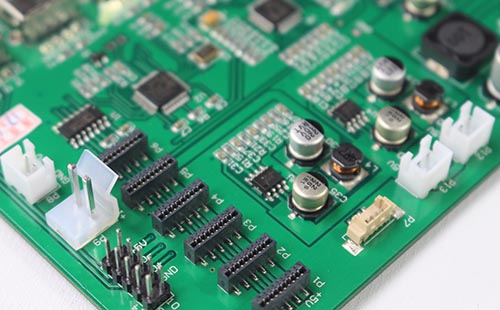
There are parasitic capacitors and parasitic inductors in the vias. In the design of high-speed digital circuits, the parasitic inductance of the vias often brings more harm than the parasitic capacitance. Its parasitic series inductance will weaken the contribution of the bypass capacitance and the filtering effectiveness of the entire power system. We can simply calculate the approximate parasitic inductance of a vias with the following formula: L=5.08h [ln (4h/d) 1], where L refers to the inductance of the vias, H is the length of the vias and d is the diameter of the central drilling hole. It can be seen from the formula that the diameter of the vias has little influence on the inductance, while the length of the vias has the greatest influence on the inductance. Still using the above example, it can be calculated that the inductance of the vias is: L=5.08x0.050 [ln (4x0.050/0.010) 1]=1.015nH. If the rise time of the signal is 1ns, The equivalent impedance is XL=π L/T10-90=3.19 Ω. Such impedance can not be ignored when there is high-frequency current passing through. Pay special attention to that the bypass capacitor needs to pass through two vias when connecting the power layer and the formation, so that the parasitic inductance of the vias will be multiplied.
From the above analysis of the parasitic characteristics of vias, we can see that in high-speed PCB design, seemingly simple vias often bring great negative effects to the circuit design. In order to reduce the adverse effects of the parasitic effects of vias, we can do as much as possible in the design:
1. In consideration of both cost and signal quality, choose a reasonable size of vias. For example, for 6-10 layers of memory module PCB design, it is better to choose 10/20Mil (drill/pad) vias. For some high-density small size boards, you can also try to use 8/18Mil vias. Under the current technical conditions, it is difficult to use smaller vias. For power or ground wire vias, you can consider using larger sizes to reduce impedance.
2. From the two formulas discussed above, it can be concluded that the use of thinner PCB is beneficial to reduce the two parasitic parameters of vias.
3. The signal wiring on the PCB shall not change layers as much as possible, that is to say, unnecessary vias shall not be used as much as possible.
4. The pins of power supply and ground shall be punched nearby. The shorter the lead between the via and pin, the better, because they will lead to an increase in inductance. At the same time, the lead between power supply and ground shall be as thick as possible to reduce impedance.
5. Place some grounded vias near the vias for signal layer change to provide the nearest circuit for the signal. You can even place a large number of redundant grounded vias on the PCB. Of course, you need to be flexible in design. The vias model discussed above is the case that each layer has pads. Sometimes, we can reduce or even remove the pads of some layers. Especially when the vias density is very large, It may lead to the formation of a slot to cut off the circuit in the copper layer. To solve this problem, in addition to moving the position of the vias, we can also consider reducing the pad size of the vias on the copper layer.


Just upload Gerber files, BOM files and design files, and the KINGFORD team will provide a complete quotation within 24h.