
Professional PCB manufacturing and assembly
Building 6, Zone 3, Yuekang Road,Bao'an District, Shenzhen, China
+86-13410863085Mon.-Sat.08:00-20:00

When designing PCB pads in progress, it is necessary to design in strict accordance with relevant requirements and standards. Because in SMT chip processing, the design of PCB pad is very important. The pad design will directly affect the solderability, stability and heat transfer of components, as well as the chip processing quality. What is the PCB pad design standard?
1、 PCB pad shape and size design standards:
1. Call PCB standard package library.
2. The minimum single side of the pad shall not be less than 0.25mm, and the maximum diameter of the entire pad shall not be greater than 3 times of the element aperture.
3. Try to ensure that the distance between the edges of two pads is greater than 0.4 mm.
4. Pads with hole diameter more than 1.2mm or pad diameter more than 3.0mm shall be designed as diamond or quincunx pads
5. In case of dense wiring, oval and oblong connecting discs are recommended. The diameter or minimum width of single panel pad is 1.6mm; For the weak current circuit pad of double-sided PCB, only the hole diameter plus 0.5mm can be used. If the pad is too large, unnecessary welding may occur.
2、 PCB pad via size standard:
The inner hole of the pad is generally not less than 0.6mm, because it is not easy to process holes smaller than 0.6mm when punching. Generally, the diameter of the metal pin plus 0.2mm is taken as the inner hole diameter of the pad. For example, when the diameter of the resistance metal pin is 0.5mm, the inner hole diameter of the pad corresponds to 0.7mm, and the diameter of the pad depends on the inner hole diameter.
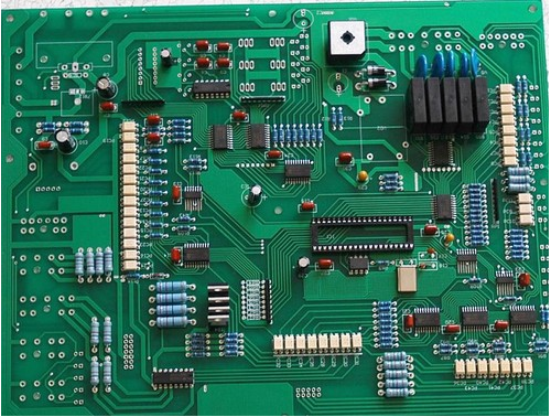
PCB design
3、 Key points of PCB pad reliability design:
1. Symmetry: To ensure the balance of the surface tension of molten solder, the pads at both ends must be symmetrical.
2. Pad spacing, too large or too small pad spacing will cause welding defects, so ensure that the spacing between PCB component ends or pins and pads is appropriate.
3. The remaining size of the pad, after the component end or pin is lapped with the pad, must ensure that the solder joint can form a meniscus.
4. The width of bonding pad shall be basically consistent with the width of component end or pin.
With correct PCB pad design, if there is a small amount of skew during chip processing, it can be corrected due to the effect of surface tension of molten solder during reflow soldering. If the PCB pad design is not correct, even if the mounting position is very accurate, it is easy to have component position offset, suspension bridge and other welding defects after reflow soldering. Therefore, great attention should be paid to PCB pad design when PCB design is carried out.


Just upload Gerber files, BOM files and design files, and the KINGFORD team will provide a complete quotation within 24h.