
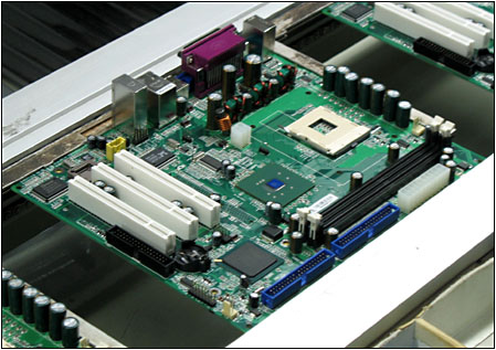
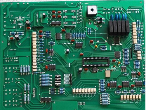
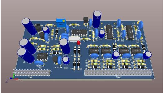
Professional PCB manufacturing and assembly
Building 6, Zone 3, Yuekang Road,Bao'an District, Shenzhen, China
+86-13410863085Mon.-Sat.08:00-20:00

1) In PCB design, the small power supply is first paved with copper on the signal layer, and then connected through PCB wiring meeting current carrying requirements;
2) PCB design 12V, 5V power supply If it is the input power supply of switching power supply, it is preferred to be disposed in the signal layer (surface layer, inner layer signal layer). If it must be divided in the plane layer, it should not be used as the reference plane for important signal lines; This can effectively reduce the impact of such "high" pressure on the signal;
3) In PCB design, if the divided power plane is used as the reference plane of the signal, the power plane is preferred as the signal reference plane of the power module; If there are multiple power supplies, the power supply with low reference voltage is preferred; For example, if the DDR3 uses a 1.5V power supply, the 1.5V power supply plane can be used as the signal reference plane of the DDR3 module, but try not to refer to the 3.3V power supply or other power supplies; (Generally, DDR3 data refers to ground plane, and address control signal refers to power plane)
4) The power plane is closely adjacent to the ground plane. If the power plane is adjacent to the signal layer, try to add more GND copper on the PCB signal layer and punch GND vias;
5) PCB design division line width should be reasonable; The width of dividing line is related to the voltage difference between two power supplies. It is generally recommended that the dividing width between modules is 25mil; The division width between numbers is 15 mils, and it can be smaller locally; The width of the split line can also be flexibly adjusted according to the space on the board, and in principle, the larger the better;
6) For PCB design, the shell ground separation width shall be 2mm in priority, and it shall be adjusted locally according to the situation. Generally, it is required to be no less than 1mm; Other signals shall be far away from the enclosure ground, including signal lines, vias, copper laying, etc;
7) In PCB design, if the power/ground plane is divided, note that the signal lines of adjacent signal layers should not be divided across, and try to avoid high-speed signal crossing on the divided reference plane.
8) The PCB design separates the power supply via from the isolation strip, and the isolation strip avoids copper, which will result in no connection of such power supply via;
9) PCB power supply in the simulated area is designed for PCB. In order to reduce the impact of power supply on signals, it is generally not recommended to lay power network copper in large areas. Generally, it is handled in the signal layer. The power supply can only be laid with copper or routed to meet the current carrying requirements, and other areas should be laid with copper and punched with ground through holes as much as possible;
10) PCB design high voltage power supply and low voltage power supply should be partitioned, and the greater the spacing, the better; Avoid high-voltage interference with low-voltage power supply and signal;
11) Common creepage avoidance spacing in PCB design:
i. When the voltage is less than 24V, the resistance welding of the surface cover shall be conducted with the spacing ≥ 0.13mm; Resistance welding without cover on the surface, spacing ≥ 0.64mm
ii. When 24V ≤ voltage < 48V, the distance between primary side ≥ 0.5mm, and the distance between secondary side ≥ 0.2mm;
Iii. When 48V ≤ voltage < 100V, spacing ≥ 1mm
Iv. When 100V ≤ voltage < 200V, spacing ≥ 1.5mm
v. When 200V ≤ voltage < 400V, spacing ≥ 2.5mm
Vi. When 400V ≤ voltage < 600V, spacing ≥ 3.2mm
vii. When the voltage is ≥ 600V, the spacing is ≥ 5mm
12) PCB design confirms that the power supply and ground can carry enough current. Whether the number of vias meets the bearing requirements
(Estimation method: 1A/mm line width when the outer copper layer is 1oz thick, 0.5A/mm line width for the inner layer)
13) PCB is designed to reduce the edge radiation effect of the plane, and the 20H principle should be met as far as possible between the power layer and the stratum.
(If conditions permit, the more indented the power layer, the better).
"" means to ensure that the edge of the power plane is indented at least 20 times as far as the edge of the ground plane (0V reference plane), where H is the distance between the power plane and the ground plane.
Why do we need the 20H principle?
In high-speed PCB, the mutual coupling of RF energy between the power plane and the ground plane usually becomes an edge flux leakage situation, and RF energy (RF current) will radiate along the PCB edge. In order to reduce this coupling effect, the physical size of all power planes should be 20H smaller than the nearest ground plane.
14) If PCB design is divided, check whether the ground to avoid division does not constitute a loop?
15) Do different power planes of adjacent layers of PCB design avoid overlapping?
16) Is the isolation between PCB design protective ground and GND greater than 4mm?
17) Is there a 10~20mm protective ground near the panel with connector in PCB design, and are the layers connected by double row staggered holes?
18) Check the effective width of PCB design power supply wiring: whether the positive and negative sheet copper is interrupted (BGA, vias are dense, and whether there is a high-speed bus at the vias are dense), focus on 0.8mmBGA.


Just upload Gerber files, BOM files and design files, and the KINGFORD team will provide a complete quotation within 24h.