
Professional PCB manufacturing and assembly
Building 6, Zone 3, Yuekang Road,Bao'an District, Shenzhen, China
+86-13410863085Mon.-Sat.08:00-20:00

Detailed explanation of PCB electromagnetic compatibility design
EMC refers to the ability of electronic equipment to work coordinately and effectively in various electromagnetic environments. The purpose of EMC design is to enable electronic equipment to suppress all kinds of external interference, enable electronic equipment to work normally in a specific electromagnetic environment, and reduce the electromagnetic interference of electronic equipment to other electronic equipment.
1. Select reasonable wire width
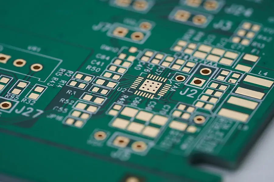
Since the impact interference caused by transient current on the printed wire is mainly caused by the inductance of the printed wire, the inductance of the printed wire should be minimized. The inductance of a printed wire is proportional to its length and inversely proportional to its width, so a short and precise wire is beneficial to interference suppression. The signal wire of clock lead, row driver or bus driver often carries large transient current, and the printed wire should be as short as possible. For discrete component circuits, when the printed wire width is about 1.5mm, the requirements can be fully met; For integrated circuits, the width of printed wire can be selected from 0.2 to 1.0mm.
2. Use the right cabling strategy
The use of equal routing can reduce the conductor inductance, but the mutual inductance and distributed capacitance between the conductors increase. If the layout allows, it is better to use the well shaped mesh wiring structure. The specific method is that one side of the printed board is wired horizontally and the other side is wired longitudinally, and then it is connected with the metal hole at the cross hole.
3. Suppress crosstalk between printed board conductors
In order to suppress the crosstalk between the wires of the printed board, long distance equal wiring shall be avoided as far as possible during the design of wiring, and the distance between wires shall be pulled as far as possible. The signal wire shall not cross with the ground wire and the power wire as far as possible. A grounded printed wire is set between some signal wires that are very sensitive to interference, which can effectively suppress crosstalk.
4. Avoid electromagnetic radiation generated when high-frequency signals pass through printed wires
In order to avoid the electromagnetic radiation generated when the high-frequency signal passes through the printed wire, the following points should also be noted when wiring the printed circuit board:
(1) The discontinuity of the printed wire shall be reduced as far as possible, for example, the wire width shall not change suddenly, the corner of the wire shall be greater than 90 degrees, and circular wiring is prohibited.
(2) The clock signal lead is most likely to generate electromagnetic radiation interference. When wiring, it should be close to the ground circuit, and the driver should be close to the connector.
(3) The bus driver shall be close to the bus to be driven. For those leads leaving the printed circuit board, the driver should be close to the connector.
(4) A signal ground wire shall be clamped between every two signal wires for data bus wiring. It is better to place the ground loop close to the least important address lead, because the latter often carries high-frequency current.
(5) When high speed, medium speed and low speed logic circuits are arranged on the printed circuit board, the devices shall be arranged in the way shown in Figure 1.
5. Suppress reflection interference
In order to suppress the reflected interference at the terminals of printed lines, except for special needs, the length of printed lines should be shortened as much as possible and slow speed circuits should be used. If necessary, terminal matching can be added, that is, a matching resistor with the same resistance value can be added at the end of the transmission line to the ground and the power supply. According to experience, for general fast TTL circuits, terminal matching measures should be taken when the printed line is longer than 10cm. The resistance value of the matching resistance shall be determined according to the maximum value of the output drive current and the absorption current of the integrated circuit.
6. Differential signal line routing strategy is adopted in circuit board design
The differential signal pairs that are very close to each other will also be closely coupled with each other. This mutual coupling will reduce EMI transmission. Generally (there are some exceptions, of course), differential signals are also high-speed signals. Therefore, high-speed design rules are generally applicable to the layout of differential signals, especially when designing the signal lines of transmission lines. This means that we must design the wiring of signal lines very carefully to ensure that the characteristic impedance of signal lines is continuous throughout the signal lines and maintains a constant.
During the placement and routing of the differential line pair, we want the two PCB lines in the differential line pair to be identical. This means that in practical application, we should try our best to ensure that the PCB lines in the differential line pair have exactly the same impedance and the wiring length is also completely consistent. Differential PCB lines are always routed in pairs, and the distance between them along the direction of the pair remains a constant at any position. In general, the layout and routing of differential line pairs are always as close as possible.


Just upload Gerber files, BOM files and design files, and the KINGFORD team will provide a complete quotation within 24h.