
Professional PCB manufacturing and assembly
Building 6, Zone 3, Yuekang Road,Bao'an District, Shenzhen, China
+86-13410863085Mon.-Sat.08:00-20:00

Circuit board design is a daily work. Although they have many years of PCB design experience, it is difficult to make high-quality PCB designs.
There are many factors to consider. Now let's discuss seven factors that need to be considered in high-quality PCB design.
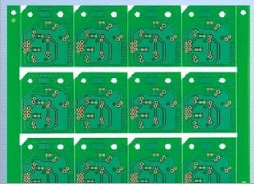
PCB design
If electronic engineers want to design high-quality circuit boards, electronic engineers or beginners should remember the following seven points.
1. PCB material: it is the foundation of any project. You need to understand how much material it takes to make a PCB.
PCB is a non-conductive solid material, which is pressed together with copper. Copper plating helps to form conductive surfaces. The basic material is generally glass reinforced FR-4 epoxy. This material is moderately priced and flame retardant.
PTFE or ceramic base used in RF or high-performance circuits for various fillers.
2. PCB stacking: PCB refers to how many layers each PCB will have. This enables electronic engineers to know the PCB impedance required for each layer. A reasonable number of layers can help engineers determine the correct manufacturing process, so as to obtain ideal output, reliability and minimize production costs.
3. Copper wire: copper wire is the most important component on PCB, and is made of copper. When designing them, be sure to understand their nature and limitations. Generally, copper wire can be produced by placing a solid metal sheet on the substrate to remove some copper.
4. Through hole type: Through holes are a key part of any PCB because they help to establish connections between different parts. You need to learn all kinds of Vias: embedded, penetrative, blind area and microcomputer (stacked, multi player and single player). For the best PCB design, the vias are small. You also need to understand the current carrying capacity of these vias.
5. Select parts: This is the most tedious step in all PCB design projects. Correct selection of parts can reduce errors and ensure the quality of PCB design. Because there are millions of components in the market, you need to remember the following:
Universal and easy to use components shall be selected. Do not use parts other than those produced.
Some products sell a lot, so you should pay attention when choosing goods.
All components adopt a packaging form to help EE connect them with PCB. Several packages can be used for some parts to make them compatible.
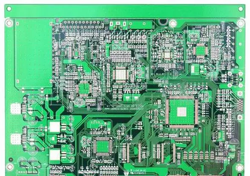
Circuit board design
6. Circuit board design rules: After meeting all the above requirements, electronic engineers should focus on the design rules. Crosstalk budget, component layout, hierarchy, time of flight analysis, production design rules and other issues should be widely considered.
7. Signal and power integrity: This is considered one of the advantages of high-quality PCB. There are many factors to consider, such as signal attenuation and rise time, driving strength, track length and characteristic impedance. To ensure quality performance, signal integrity (SI) simulation will be performed before and after PCB layout. Efficient circuits require high currents. Therefore, AC and DC performance of distribution network shall be considered


Just upload Gerber files, BOM files and design files, and the KINGFORD team will provide a complete quotation within 24h.