
Professional PCB manufacturing and assembly
Building 6, Zone 3, Yuekang Road,Bao'an District, Shenzhen, China
+86-13410863085Mon.-Sat.08:00-20:00

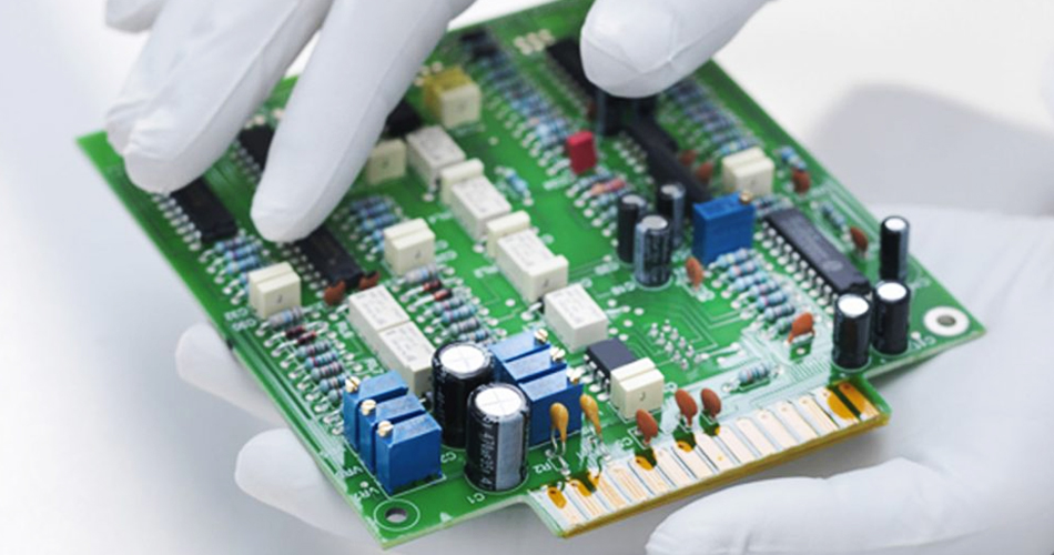
PCBA electronic engineers must know the installation principles of PCB components
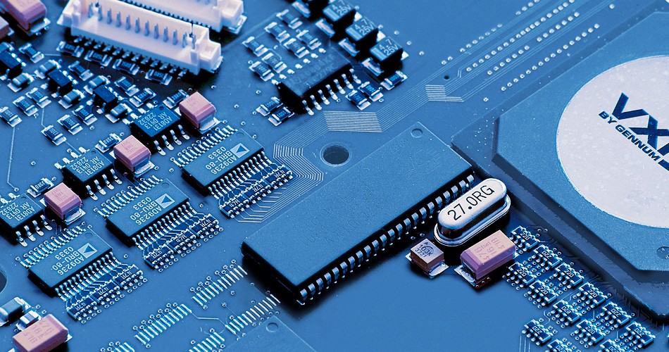
How much do you know about the insertion of electronic components on PCB? Now the insertion of electronic components is very particular, and the key points and principles to be paid attention to are also very complicated. Today we will introduce the insertion methods and process requirements of circuit board components. The insertion of components is a process and procedure. In addition to affecting the orderly and beautiful arrangement of components on the installed circuit board, it is more important that the installation of components directly affects the installation quality of the circuit board. Therefore, there are strict requirements for the insertion of components.
(1) The installation and insertion of components should follow the principle of "big first, small second, low first, high second, inside first, outside first", which is conducive to the smooth installation and insertion.
(2) When the resistance element is installed horizontally, the mark number shall be upward and the direction shall be consistent. Those with low power can be installed and inserted close to the plane of the printed circuit board, while those with high power should be 2mm away from the plane of the printed circuit board, which is helpful for heat dissipation of components.
(3) When the capacitors, triodes and other components are installed and inserted stereoscopically, the lead wire cannot be kept too long, otherwise the stability of the components will be reduced; However, it should not be too short to avoid damage to components due to overheating during welding. Generally, it is 2mm away from the circuit board, and pay attention to the positive and negative polarity of the electrolytic capacitor and the pins of the triode.
(4) The insertion of components on the printed circuit board shall be evenly distributed, neatly arranged and beautiful, and shall not be inclined, crossed or overlapped. The shell of components and leads shall not touch each other, and a certain distance shall be reserved.
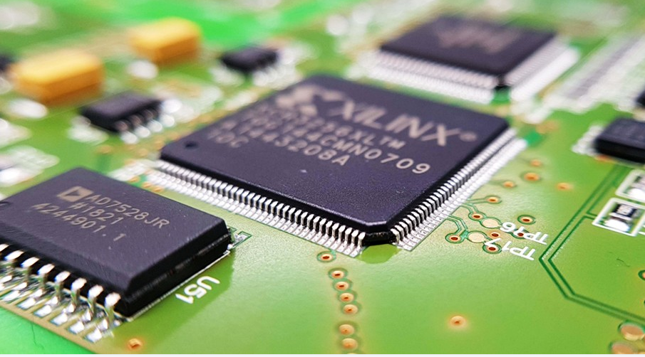
Installation principle of PCB components. For some new electronic engineers, this problem is somewhat complicated, and may even be mistaken for something that can only be understood by professionals. In fact, it is not. The installation principles of PCB components are not so complicated and difficult to understand as everyone imagined. Today, let's take a look at the installation principles of PCB components.
Installation principle of PCB components:
1. The components shall be arranged inside the PCB board, and each lead out pin of the components shall occupy a bonding pad separately.
2. Components cannot occupy the whole PCB panel, and 5~10mm margin shall be left around the board. The size of PCB area and fixing method determine the margin around the board.
3. Components and parts shall be laid evenly and uniformly throughout the layout.
4. The installation height of components should be as low as possible. If it is too high, it is easy to fall over or adjacent components are connected, which may lead to poor safety performance of the system.
5. The axial position of the larger component is determined by the installation status of the printed circuit board in the system. The axis direction of the regularly arranged components should be in the vertical direction in the system, so as to improve the stability of the components on the PCB.
6. The span at both ends of the component shall be slightly greater than the axial length of the component. When bending the pins, do not bend them all, but leave a distance of about 2mm to avoid damaging the components.
7. The layout of components shall not be crossed up and down. A certain distance shall be kept between adjacent components, and the spacing shall not be too small.


Just upload Gerber files, BOM files and design files, and the KINGFORD team will provide a complete quotation within 24h.