
Professional PCB manufacturing and assembly
Building 6, Zone 3, Yuekang Road,Bao'an District, Shenzhen, China
+86-13410863085Mon.-Sat.08:00-20:00

1. Print the circuit board. The painted circuit board is printed out with transfer paper, pay attention to the slippery side facing yourself, generally print two boards, that is, print two boards on a piece of paper. Select the best printing effect in the production of PCB circuit boards.
2. Cut the copper-clad plate, and use the photosensitive plate to make the whole circuit board diagram. Copper clad plate, that is, a circuit board covered with copper film on both sides, cut the copper clad plate into the size of the PCB board, not too large, to save materials.
3, pretreatment of copper clad plate. Use fine sandpaper to polish off the oxide layer on the surface of the copper-clad plate to ensure that the carbon powder on the thermal transfer paper can be firmly printed on the copper-clad plate when transferring the circuit board. The standard for polishing is that the surface of the board is bright and there is no obvious stain.

4. Transfer circuit board. The printed circuit board is cut to the appropriate size, the printed side of the circuit board is attached to the copper clad plate, and the copper clad plate is placed into the heat transfer machine after alignment, and the transfer paper must be ensured that there is no dislocation. Generally speaking, after 2-3 transfers, the circuit board can be firmly transferred to the copper-clad plate. The heat transfer machine has been preheated in advance, the temperature is set at 160-200 degrees Celsius, due to the high temperature, pay attention to safety when operating!
5, corrosion circuit board, reflow welding machine. First check whether the circuit board transfer is complete, if there are a few no transfer place can be repaired with black oil pen. Then it can be corroded, and when the exposed copper film on the circuit board is completely corroded away, the circuit board is removed from the corrosive liquid and cleaned, so that a circuit board is corroded well. The corrosive liquid is composed of concentrated hydrochloric acid, concentrated hydrogen peroxide, water, the ratio is 1:2:3, in the preparation of corrosive liquid, first put water, and then add concentrated hydrochloric acid, concentrated hydrogen peroxide, if the operation of concentrated hydrochloric acid, concentrated hydrogen peroxide or corrosive liquid accidentally splashed on the skin or clothing should be cleaned with water in time, because the use of strong corrosive solution, the operation must pay attention to safety!
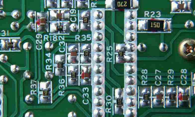
6, PCB board drilling. The PCB board is to insert electronic components, so it is necessary to drill the PCB board. Select different drilling needles according to the thickness of the electronic component pin. When using the drilling rig to drill, the circuit board must be stable, and the drilling rig speed cannot be opened too slowly. Please carefully watch the operation of the operator. ?
7, PCB circuit board pretreatment. After drilling, polish off the toner covered on the circuit board with fine sandpaper, and clean the PCB board with water. After the water is dried, apply the rosin water on the side with the line, in order to speed up the rosin solidification, we use a hot fan to heat the circuit board, and the rosin can solidify in only 2-3 minutes.
8. Weld electronic components. After welding the electronic components on the plate, power.
Analyze the design principle of mixed signal PCB board
The operation of analog circuits depends on continuous changes in current and voltage. The operation of a digital circuit depends on the detection of a high or low level at the receiving end according to a pre-defined voltage level or threshold, which is equivalent to determining the "true" or "false" logic state. Between the high and low levels of a digital circuit, there is a "gray" area where the digital circuit sometimes displays analog effects, such as when jumping from a low level to a high level (state), if the digital signal jumps fast enough, there will be overrush and backring reflections.
For modern board design, the concept of mixed-signal PCBS is ambiguous, because even in purely "digital" devices, there are still analog circuits and analog effects. Therefore, in the early stage of the design, simulation of the simulation effect must be carried out in order to reliably achieve strict timing allocation. In fact, in addition to communication products that must have the reliability to work for years without failure, simulation of simulation effects is particularly required in mass-produced low-cost/high-performance consumer products.
Another difficulty of modern mixed-signal PCB design is the increasing number of devices with different digital logic, such as GTL, LVTTL, LVCMOS and LVDS logic, each logic circuit has different logic thresholds and voltage swings, but these different logic thresholds and voltage swings must be designed together on a PCB. Here, you can master the strategies and techniques for success by thoroughly analyzing the layout and routing design of high-density, high-performance, mixed-signal PCBS.
First, the basis of mixed signal circuit wiring
When digital and analog circuits share the same components on the same board, the layout and wiring of the circuit must be methodical. The matrix shown in Figure 1 is helpful for the design planning of a mixed-signal PCB. Only by revealing the characteristics of digital and analog circuits can the required PCB design objectives be achieved in the actual layout and routing.
In mixed-signal PCB design, there are special requirements for power wiring and analog noise and digital circuit noise are required to be isolated from each other to avoid noise coupling, so that the complexity of layout and wiring is increased. The special requirements for power transmission lines and the need to isolate noise coupling between analog and digital circuits add further complexity to the layout and routing of mixed-signal PCBS.
If the power supply of the analog amplifier and the digital power supply of the A/D converter are connected together, it is likely to cause the interaction of the analog part and the digital part of the circuit. Perhaps, because of the position of the input/output connectors, the layout scheme must mix the wiring of the digital and analog circuits.
Before the layout and wiring, engineers need to figure out the basic weaknesses of the layout and wiring scheme. Even in the presence of false judgments, most engineers tend to use layout and wiring information to identify potential electrical effects.
Second, the layout and wiring of modern mixed-signal PCB
The following will elaborate the mixed-signal PCB manufacturing layout and routing technology through the design of the OC48 interface card. OC48 stands for optical carrier Standard 48, which is basically for 2.5Gb serial optical communication, and it is a kind of high-capacity optical communication standard in modern communication equipment. The OC48 interface card contains several typical mixed-signal PCB layout and routing problems, the layout and routing process will indicate the sequence and steps to solve the mixed-signal PCB layout solution.


Just upload Gerber files, BOM files and design files, and the KINGFORD team will provide a complete quotation within 24h.