
Professional PCB manufacturing and assembly
Building 6, Zone 3, Yuekang Road,Bao'an District, Shenzhen, China
+86-13410863085Mon.-Sat.08:00-20:00

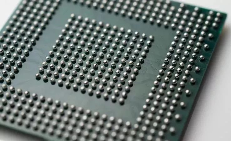
BGA components and their assembly process
(1) Visual inspection
For package arrays such as BGA, without inspection equipment, first visually observe whether the collapse of the outermost solder joints is consistent, and then look at the chip against the light. If each row and column can transmit light , then it can be concluded that there is no continuous soldering, and sometimes larger solder balls can also be seen. However, internal defects such as voids cannot be detected.
(2) Appearance visual optical inspection system
At the heart of the system is a two-component head, shown in Figure 5, consisting of a fiber optic light source and an optics head mounted on a very precise X/Y plate, beneath which the PCB board to be inspected is placed. When inspecting, the head is lowered to the part with the magnifying glass on one side of the part and the light source on the other side backlit. Solder joints are inspected by going row by row along the part. Interconnects can be seen and evaluated by adjusting the field of view. All of this is projected onto a flat-screen monitor by a high-resolution CCD color camera integrated in the microscope.
(3) Electrical test and boundary scan detection
Traditional electrical testing is the primary method for finding opens and shorts. Its sole purpose is to make the actual electrical connections at preset points on the board, thus providing an interface for signals to flow into the test board and data to flow into the ATE. The system can also check the functionality of the device if the printed circuit board has enough space for test points. The test instrument is generally controlled by a microcomputer, and the corresponding needle bed and software are required to detect each PCB. For different test functions, the instrument can provide corresponding working units for detection, such as DC level unit for testing diodes and triodes; AC unit for testing capacitance and inductance; High frequency signal unit.
Boundary-scan technology addresses some of the issues associated with complex devices and packaging densities. Using boundary scan technology, each IC device is designed with a series of registers to separate the functional circuit from the detection circuit and record the detection data passing through the device. The test path checks the open circuit and short circuit of each solder joint on the IC device. Based on the detection port of the boundary scan design, each solder joint is provided with a path through the edge connector, thereby eliminating the need for a full node lookup. Although boundary scan provides a wider inspection range of invisible solder joints than electrical testing, printed circuit boards and IC devices must also be specially designed for scanning inspection.
Electrical testing and boundary scan testing are mainly used to test electrical properties and determine whether the conductive current is on or off, but they cannot better detect welding quality. If assisted by non-physical solder joint testing, it will help to improve the assembly process and SPC (statistical process control).
(4) X-ray test
There are very few inspection equipment that can be used for accurate measurement and quality inspection of the entire BGA device assembly process. Automated laser inspection equipment can test the deposition of solder paste before component placement, but they are slow and cannot be used Inspect BGA device solder joint defects. Acoustic microscopy is used to inspect BGA solder joints of polyimide and ceramic packages, but cannot detect BGA solder joints of BT resin material packages. X-ray fluoroscopy can show weld thickness, shape and mass density distribution. Thickness and shape are not only indicators of long-term structural quality, but are also good indicators of open and short defects and insufficient welds. This technique helps to collect quantified process parameters and detect defects.
X-ray image detection principle: X-rays are generated by a micro-focus X-ray tube, pass through a beryllium window in the tube, and project onto the experimental sample. The absorption or transmission of X-rays by a sample depends on the composition and ratio of the materials contained in the sample. X-rays passing through the sample strike a phosphor-coated image detector and excite photons, which are then detected by a camera, which then processes and amplifies the signal for further analysis by a computer.
Different sample materials have different absorption rates for X-rays (see Table 7), and the processed grayscale images show differences with the density of the object being inspected or the thickness of the material.
Table 7 Opacity coefficients of different materials to X-rays
Material
use
Absorption rate
plastic
Package
extremely small
gold
Chip wire bonding
very high
lead
solder
high
aluminum
Die wire bonding, heat sink
extremely small
tin
solder
high
copper
PCB printed line
medium
epoxy resin
PCB substrate
extremely small
Silicon
Semiconductor chip
extremely small
l Artificial X-ray inspection
Using manual X-ray inspection equipment, it is necessary to check the solder joints one by one and determine whether they are qualified. The equipment is equipped with manual or computer aids for better inspection and videography. Detailed defined standards or visual inspection charts guide the evaluation of inspection results. The usual visual inspection requires training of operators, and is prone to errors, and manual equipment is not suitable for testing all solder joints, only suitable for process identification and process failure analysis.
l Automatic X-ray inspection
The automatic detection system can detect all solder joints, and is usually used in production equipment with high output and few varieties. Products with high value or reliability requirements also need automatic detection. The test results are sent to the repair personnel together with the circuit boards that need to be repaired, and relevant statistical data are provided to improve the production process.
The automatic detection system needs to set the correct detection parameters. The detection index is defined in the software of most new systems, but it must be re-formulated to define the area and height of the solder joint to be inspected or to cut the solder joint into different cross-sections to adapt to the unique factors in the production process, otherwise it may get wrong information and reduce system reliability.
The automatic detection system has two working modes: direct X-ray test system and section X-ray automatic test system. The direct X-ray system is derived from the compound absorption characteristics of the X-ray beam along the path. For some SMT soldering, such as J-type leads and fine-pitch QFP on a single-sided PCB, it is the best method to measure the soldering quality, and the equipment Cheaper, but it cannot distinguish vertically overlapping features. When there are components at the same position on both sides of the PCB, the shadows formed by these solders will overlap, and it is difficult to distinguish which layer is the problem; in addition, when the solder seam of the BGA device is covered by its internal leads, the above-mentioned problem also exists. question. The cross-sectional X-ray test system overcomes these problems by designing a focused cross-section and separating the horizontal areas of the PCB by defocusing the upper and lower planes of the target area. The system's success lies in its ability to accurately detect welding defects with only a short test time. For complex products with small volumes, it is best to use a cross-sectional X-ray testing system. While all methods can inspect solder joints, cross-sectional X-ray testing systems provide a non-destructive testing method to detect the quality of all types of solder joints and obtain valuable information for adjusting the assembly process.
l Cross-section X-ray automatic test
The tomographic profile measures 4 fundamental physical parameters of each "slice": the center position of the solder joint, the diameter of the solder joint, the respective solder thicknesses of the 5 rings coaxial with the center of the solder joint, the solder joint relative to the known circle degree of circular shape error.
The relative position of the solder joint center position in different slice images indicates the displacement of the BGA device on the PCB pad; the solder joint diameter measurement indicates the relative amount of solder in the solder joint compared with the standard solder volume; The diameter measurement of the diameter indicates an open circuit caused by solder paste printing or pad contamination, while the diameter measurement at the solder ball indicates the joint coplanarity, and the solder thickness measurement of each coaxial ring and its rate of change. Judging the distribution of solder in the solder joint is more effective in determining poor wetting and porosity defects. The roundness of the solder joint indicates the uniformity of the solder distribution around the solder joint compared with the standard circle, which provides data for judging device displacement and solder joint wetting.
The amount of solder and its distribution at the connection point, through two or more different heights on the BGA solder joint (such as the printed circuit board pad contact surface, component contact surface, or component and printed circuit Half the height between boards), direct measurements of cross-sectional images or "horizontal slices" combined with multiple slice measurements of similar BGA joints effectively provide three-dimensional testing. Within each cross-sectional X-ray image "slice" of the conventional structure of BGA joints, specific joint features are isolated and measured to provide quantitative Statistical Process Control (SPC) measurements, which can Used to track process excursions and characterize them into corresponding defect categories.
BGA Reliability Impact
Jun 05,2023


Just upload Gerber files, BOM files and design files, and the KINGFORD team will provide a complete quotation within 24h.