
Professional PCB manufacturing and assembly
Building 6, Zone 3, Yuekang Road,Bao'an District, Shenzhen, China
+86-13410863085Mon.-Sat.08:00-20:00

The difference between PCB circuit and chip circuit
Difference: PCB is a printed circuit board; IC is an integrated circuit. An integrated circuit is a general-purpose circuit integrated into a chip. It is a whole. Once it is damaged inside, the chip will also be damaged. The PCB can solder the components by itself, and the components can be replaced if it is broken. IC board: generally the carrier board on the chip, the board is very small, generally 1/4 the size of a fingernail, the board is very thin 0.2~0.4mm, the material used is FR-5, BT resin, and its circuit is 2mil/2mil about. For high-precision boards, they were generally produced in Taiwan in the past, and now they are developing to the mainland. The yield rate in the industry is 75%. The unit price of this kind of board is very high, and it is usually bought by PCS. PCB board: it is our mobile phone, computer and peripheral boards, including N-BOOK board, memory stick, LCD, H-DI and other boards. Features: the board is generally around 1.0, and the line is 4mil/4mil (I can’t do it 2/2 , The process is different) The material is mostly FR-4, epoxy resin, now it belongs to cabbage, generally sold according to the area, how much is a FT. The yield rate is generally above 90%, and those below this yield rate may lose money. Generally good factories achieve 98%. A PCB board refers to a printed circuit board, while a chip is a component. The chip needs an auxiliary circuit, and after being drawn into a circuit board, all the components are soldered to realize the function of the chip. So the circuit board is equivalent to a carrier to realize the function of the chip. At present, there are many kinds of software for drawing circuit boards. We can choose one according to our own needs, and keep in touch to achieve proficiency.
The structure and manufacturing process of PCB and chip do have similarities, including features such as multilayer structure and interlayer interconnection. However, PCBs and chips have very different functions, features, and applications, so they should not be confused or mixed. In modern microelectronics technology, multiple chips are combined into a system to form a larger and more complex integrated circuit. This integrated circuit is called a "system chip" (System-on-Chip, SOC). This technology realizes the high integration and complexity of large-scale semiconductor integrated circuits, and has unparalleled performance and volume advantages. Although conceptually, adding well and inversion layers to the underside of a PCB might convert it into a large system-on-a-chip, from a practical manufacturing and application point of view, this approach presents several insurmountable problems. For example: the specific manufacturing process is different: the manufacturing process and process equipment of PCB and integrated circuit are different, and require different process flow and manufacturing environment. Processes such as solid substrates, mask lithography, chip packaging, and thermal annealing all have special properties compared to PCB manufacturing. There are differences in design, simulation, and verification: chip design and PCB design are different and have their own design tools, specifications and processes. And the design, simulation and verification process of the system chip is considered to be more complex and systematic than the PCB design. Huge difficulty in production in terms of cost and time: The cost and time of manufacturing a large system chip will be significantly higher than PCB production, mainly because the process precision and manufacturing complexity of the finished product are usually higher than the traditional PCB manufacturing process.
 1. The printed circuit board (referred to as PCB) is a finished board with insulating substrates and conductors as materials, designed and made of printed circuits, printed components or a combination of the two according to the pre-designed circuit schematic diagram. Its main function is to use the base insulating material to isolate the copper foil conductive layer on the surface, realize the interconnection and relay transmission between electronic components, and make the current amplify and attenuate in various electronic components along the preset line , modulation, decoding, encoding and other functions to realize the interconnection and relay transmission between electronic components. the
2. The classification of PCB can be divided into rigid board, flexible board and rigid-flex board according to the bending toughness of the substrate used; according to the material, it can be divided into: organic board (phenolic resin, glass fiber/epoxy resin, Polyimide, BT, etc. ) and inorganic boards (aluminum substrates, copper substrates, ceramic substrates mainly depend on heat dissipation).
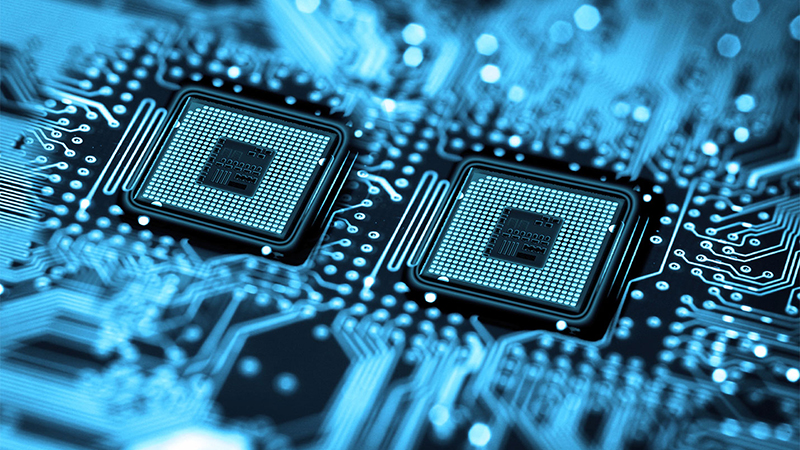
3. Characteristics of integrated circuits Integrated circuits have the advantages of small size, light weight, fewer lead wires and welding points, long life, high reliability, and good performance. At the same time, they are low in cost and convenient for mass production. It is not only widely used in industrial and civilian electronic equipment such as radio recorders, televisions, computers, etc., but also in military affairs, communications, remote control, etc. Using integrated circuits to assemble electronic equipment can increase the assembly density by tens to thousands of times compared with transistors, and the stable working time of equipment can also be greatly improved.
4. The main components of the current circuit board (1) Circuits and graphics: The circuit is used as a tool for conducting between components. In the design, a large copper surface is additionally designed as a grounding and power supply layer. Lines and drawings are made at the same time. (2) Dielectric layer: used to maintain the insulation between lines and layers, commonly known as the base material. (3) Hole: The via hole can make the lines of more than two levels conduct with each other. The larger via hole is used as a component plug-in. In addition, there are non-conducting holes, which are usually used for surface mount positioning and fixed during assembly. For screws. (4) Solder Resist Ink: Not all copper surfaces need to be tinned, so the non-tinned area will be printed with a layer of material (usually epoxy resin) that isolates the copper surface from eating tin, to avoid non-tinned areas Short circuit between lines. According to different processes, it is divided into green oil, red oil and blue oil, among which green oil is the most common. (5) Silk screen: This is a non-essential component, the main function is to mark the name and position frame of each part on the circuit board, which is convenient for maintenance and identification after assembly. (6) Surface treatment: Since the copper surface is easily oxidized in the general environment, it cannot be tinned (poor solderability), so the copper surface to be tinned will be protected. The protection methods include spraying tin, chemical gold, chemical silver, and chemical tin organic flux. Each method has its own advantages and disadvantages, and they are collectively referred to as surface treatment.
Five, PCB board characteristics (1) can be high-density. For decades, the high density of printed boards has been able to develop with the improvement of integrated circuit integration and the advancement of mounting technology. (2) High reliability. Through a series of inspections, tests and aging tests, the PCB can be guaranteed to work reliably for a long time (use period, generally 20 years). (3) Designability. For various performance (electrical, physical, chemical, mechanical, etc.) requirements of PCB, printed board design can be realized through design standardization, standardization, etc., with short time and high efficiency. (4) Manufacturability. With modern management, standardization, scale (quantity), automation and other production can be carried out to ensure the consistency of product quality. (5) Testability. A relatively complete test method, test standard, various test equipment and instruments have been established to detect and identify the qualification and service life of PCB products. (6) Assemblability. PCB products are not only convenient for standardized assembly of various components, but also can be automated and large-scale mass production. At the same time, PCB and various component assembly components can also be assembled to form larger components, systems, and even complete machines. (7) Maintainability. Since PCB products and various component assembly parts are designed and produced in a standardized manner, these parts are also standardized. Therefore, once the system fails, it can be replaced quickly, conveniently and flexibly, and the system can be restored quickly. Of course, more examples can be given. Such as making the system miniaturized and lightweight, and high-speed signal transmission. 6. The relationship and difference between PCB board and integrated circuit The integrated circuit is welded on the PCB board; the PCB board is the carrier of the integrated circuit, and the PCB board is the printed circuit board. Printed circuit boards appear in almost every electronic device. If there are electronic parts in a certain device, printed circuit boards are mounted on PCBs of various sizes. In addition to fixing various small parts, the main function of the printed circuit board is to electrically connect the various parts on it. Integrated circuits generally refer to the integration of chips, such as the chips on the motherboard and inside the CPU, are called integrated circuits. The printed circuit refers to the circuit boards we usually see, as well as printing and welding chips on the circuit board.
What is the FR4 material in PCB
May 31,2023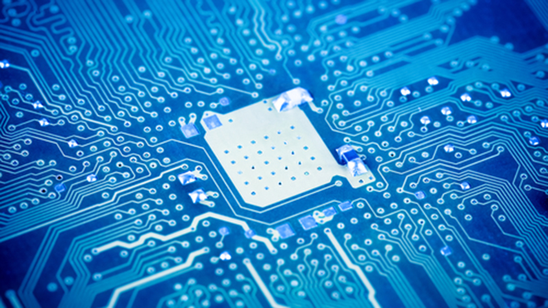


Just upload Gerber files, BOM files and design files, and the KINGFORD team will provide a complete quotation within 24h.