
Professional PCB manufacturing and assembly
Building 6, Zone 3, Yuekang Road,Bao'an District, Shenzhen, China
+86-13410863085Mon.-Sat.08:00-20:00

PCB processing process
Circuit design skills PCB design process The general PCB basic design process is as follows: preliminary preparation -> PCB structure design -> PCB layout -> wiring -> wiring optimization and silk screen -> network and DRC inspection and structural inspection -> plate making.
First: pre-preparation. This includes preparing component libraries and schematics. "If a craftsman wants to be good at his work, he must first sharpen his tools." To make a good board, in addition to designing the principle well, it is also necessary to draw well. Before PCB design, the component library of the schematic diagram SCH and the component library of the PCB must be prepared first. The component library can use the library that comes with peotel, but it is difficult to find a suitable one in general. It is best to make the component library by yourself based on the standard size data of the selected device. In principle, make the PCB component library first, and then the SCH component library. The component library requirements of PCB are relatively high, which directly affects the installation of the board; the component library requirements of SCH are relatively loose, as long as the pin attributes and the corresponding relationship with PCB components are well defined. PS: Watch out for hidden pins in the standard library. After that is the design of the schematic diagram, and when it is done, it is ready to start the PCB design.
Second: PCB structure design. In this step, according to the determined circuit board size and various mechanical positioning, the PCB board surface is drawn in the PCB design environment, and the required connectors, buttons/switches, screw holes, assembly holes, etc. are placed according to the positioning requirements. And fully consider and determine the wiring area and non-wiring area (such as how much area around the screw hole belongs to the non-wiring area).
Third: PCB layout. To put it bluntly, the layout is to put devices on the board. At this time, if the preparations mentioned above are all done, you can generate the netlist (Design->CreateNetlist) on the schematic diagram, and then import the netlist (Design->LoadNets) on the PCB diagram. I saw all the components piled up, and there were flying wires between the pins to indicate the connection. Then you can place the device. The general layout is carried out according to the following principles:
①. According to the reasonable division of electrical performance, it is generally divided into: digital circuit area (that is, fear of interference and interference), analog circuit area (fear of interference), and power drive area (interference source); ②. Circuits that complete the same function should be placed as close as possible, and each component should be adjusted to ensure the simplest connection; at the same time, adjust the relative position of each functional block to make the connection between the functional blocks the simplest; ③. For components with high mass, the installation position and installation strength should be considered; heating components should be placed separately from temperature sensitive components, and heat convection measures should also be considered if necessary; ④. The I/O drive device should be as close to the edge of the printed board as possible, and close to the lead-out connector; ⑤. The clock generator (such as: crystal oscillator or clock oscillator) should be as close as possible to the device that uses the clock; ⑥. Between the power input pin of each integrated circuit and the ground, a decoupling capacitor (generally a monolithic capacitor with good high-frequency performance is used); when the circuit board space is dense, a decoupling capacitor can also be added around several integrated circuits. Tantalum capacitors. ⑦. A discharge diode (1N4148 is enough) should be added to the coil of the relay; ⑧. The layout requirements should be balanced, dense and orderly, not top-heavy or heavy-headed
——Special attention should be paid to the actual size (area and height) of the components and the relative position between the components when placing the components, so as to ensure the electrical performance of the circuit board and the feasibility of production and installation At the same time as convenience, it should ensure that the above principles can be reflected
Under the premise, the placement of devices should be properly modified to make them neat and beautiful. For example, the same devices should be placed neatly and in the same direction, and cannot be placed in a "staggered order". This step is related to the overall image of the board and the difficulty of the next step of wiring, so it takes a lot of effort to consider. When laying out, you can make preliminary wiring for places that are not sure, and give full consideration.
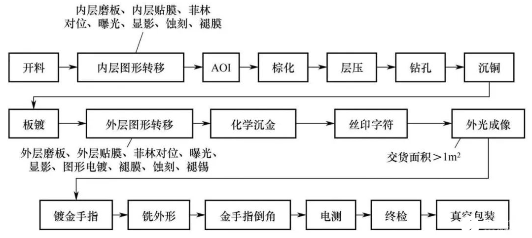
Double-sided panel: material cutting---graphic transfer---etching-drilling-copper plating-green oil characters---surface treatment-shape processing-packaging
Multi-layer board: material cutting---inner layer graphics transfer-inner layer etching-core board punching---browning and pressing-drilling-copper plating-outer layer graphics transfer-outer layer Etching --- green oil characters --- surface treatment -- shape processing -- packaging
These are general processes. If the board has special requirements, special processes are required, such as plated holes, HDI, selection of immersion gold, gold fingers, back drilling process, etc.


Just upload Gerber files, BOM files and design files, and the KINGFORD team will provide a complete quotation within 24h.