
Professional PCB manufacturing and assembly
Building 6, Zone 3, Yuekang Road,Bao'an District, Shenzhen, China
+86-13410863085Mon.-Sat.08:00-20:00

The calculation of SMT chip processing points is the main basis for the calculation of processing costs. Many customers who have only come into contact with the SMT processing industry do not know how to calculatethe price. The following professional SMT processing factory Pet Electronics will give you a brief introduction.
The current pricing in the processing industry is not uniform, and it is difficult to unify, but the general unit price range is 0.008~0.02 yuan/solder spot for SMT processing. Even the charges of the same SMT processing factory are different, mainly due to the process, Processing quantity, PCBA processing difficulty and other aspects are related.
The following is a brief introduction to the impact of different factors on valuation:
SMT patch processing Process:
1. The leaded process is generally cheaper than the lead-free process, mainly due to the difference in solder paste cost and process.
2. The price of SMT patch processingorders with solder paste red glue dual process will be slightly more expensive, because the process is relatively troublesome.
SMT patch processing Quantity:
1. In the actual SMT chip processing, the orders with small quantities will generally charge engineering fees for those orders that will lose money based on points, or directly calculate according to the minimum consumption instead of charging by points. Pater Electronics is for small batches Or the minimum consumption for proofing is probably in the range of 600-2000 yuan according to the difficulty of the board.
2. Small batch SMT processing but the quantity cannot be completely settled by the start-up fee, but the number of SMT factories is calculated by the start-up fee + point billing method, Pete Electronics generally calculates according to the minimum consumption, and will not extra Calculation of points, when the point fee exceeds the minimum consumption, it will be charged directly by point calculation, and no additional startup fee will be added.
3. Batch SMT chip processing is calculated by multiplying the calculation points by the unit price.
PCBA Difficulty
1. The cost of single-sided panels is generally lower than that of double-sided panels, because double-sided panels need to be pasted twice, and the requirements for the size of the steel mesh are relatively high.
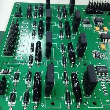
2. The cost of SMT processing with high precision requirements will be slightly higher, such as PCBA board processing with BGA and other components.
3. The calculation cost of PCBA processing points with higher density will be slightly lower, because there are more points in the PCB board of the same size, and the efficiency will be higher.
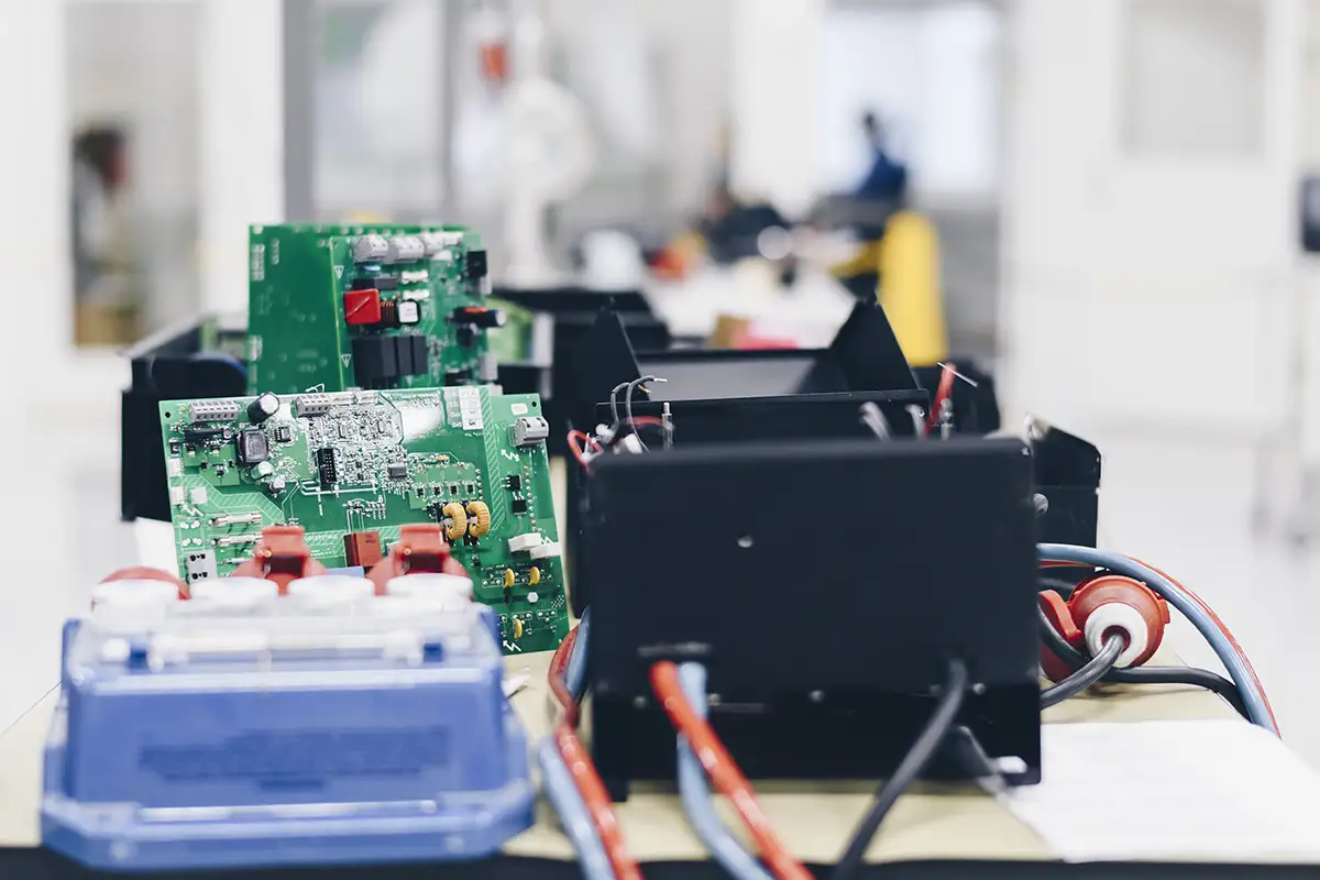
Shenzhen Kingford Technology Co., Ltd. provides professional electronic OEM processing, professional one-stop PCBA processing, SMT processing factory, provides electronic OEM processing, PCBA OEM material, professional PCBA factory . In order to allow us to develop better and learn more about product device information, the company specially arranged for us to go to the raw material supplier to learn the process flow of SMT placement. The sharing information is as follows:
SMT is Surface Mount Technology (Surface Mount Technology) (abbreviation of Surface Mounted Technology), which is currently the most popular technology and process in the electronics assembly industry. SMT patch refers to the abbreviation of a series of process processes processed on the basis of PCB. PCB (Printed Circuit Board) means printed circuit board.
SMT patch processing process:
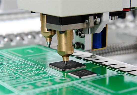
SMT basic process components: Solder paste printing --> parts mounting --> furnace curing --> reflow soldering --> AOI optical inspection --> maintenance --> board separation --> grinding board --> cleaning plate.

1. Solder paste printing: Its function is to print the solder-free paste onto the pad of the PCB to prepare for the soldering of components. The equipment used is a screen printing machine, which is located at the forefront of the SMT production line.
2. Parts mounting: Its function is to accurately install the surface mount components to the fixed position of the PCB. The equipment used is a placement machine, which is located behind the screen printing machine in the SMT production line.
3. Furnace curing: Its function is to melt the adhesive, so that the surface mount components and the PCB board are firmly bonded together. The equipment used is a curing oven, which is located behind the placement machine in the SMT production line.
4. Reflow soldering: Its function is to melt the solder paste, so that the surface mount components and the PCB board are firmly bonded together. The equipment used is a reflow oven, which is located behind the placement machine in the SMT production line.
5. AOI optical inspection: Its function is to inspect the welding quality and assembly quality of the assembled PCB board. The equipment used is automatic optical inspection (AOI), and the order quantity is usually more than tens of thousands, and the small order quantity is manually inspected. The location can be configured in a suitable place on the production line according to the needs of detection. Some are before reflow soldering, some are after reflow soldering.
6. Maintenance: Its function is to repair the PCB board that has failed. The tools used are soldering iron, rework station, etc. Configured after AOI optical inspection.
7. Split board: Its function is to split the multi-connected board PCBA so that it can be separated to form a single individual. Generally, V-cut and machine cutting are used.
8. Grinding plate: Its function is to grind the burr parts to make them smooth and flat.
9. Board washing: Its function is to remove the welding residues harmful to human body on the assembled PCB board, such as flux. It is divided into manual cleaning and washing machine cleaning, and the location may not be fixed, online or offline.
Advantages of SMT patch processing:
High assembly density, small size and light weight of electronic products.
High reliability and strong earthquake resistance. Solder joint defect rate is low.
Good high frequency characteristics. Reduced electromagnetic and radio frequency interference.
Easy to automate and improve production efficiency. Reduce costs by 30% to 50%. Save material, energy, equipment, manpower, time, etc.
It is precisely because of the complexity of the process of SMT chip processing that there have been many SMT chip processing factories, specializing in SMT chip processing. In Shenzhen, thanks to the vigorous development of the electronics industry, SMT chip processing has achieved great success. the prosperity of an industry.


Just upload Gerber files, BOM files and design files, and the KINGFORD team will provide a complete quotation within 24h.